A voltage regulator module (VRM) is a specialized point-of-load (PoL) power converter, sometimes called a processor power module (PPM). Like other PoLs, VRMs are buck converters. They are specifically designed to convert a 5V or 12V bus to a specific voltage needed to power a central processing unit (CPU) or graphics processing unit (GPU) in a computer or server. VRMs support the needs of CPUs and GPUs for low noise margins, stable voltage regulation, and fast dynamic response.
Most VRMs are multiphase (also called multistage) synchronous buck designs. The low-side synchronous MOSFET and the inductor provide feedback for regulation. VRMs usually have large banks of capacitors to stabilize the voltage and support the dynamic power needs of the CPU/GPU.
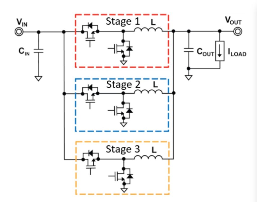
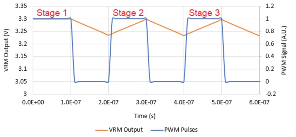
A multiphase VRM consists of a series of paralleled buck power stages (phases), each with its own inductor and power MOSFETs, driven by a single controller. While the controller in a PoL simply controls the operation of the power stages, a VRM controller also communicates with the CPU/GPU. Multiphase VRMs can have 12 or more phases that share input and output capacitors. The phases are interleaved, which means that they are switched at intervals equal to 360° / n throughout the switching period, where n is the total number of phases. The higher the required load current, the larger the number of phases. In addition, interleaving more phases effectively increases the operating frequency of the converter.
VRMs take various physical forms; some are implemented with discrete components on the motherboard, some separate modules that plug into a dedicated connector on the motherboard, and some are integrated directly into the CPU/GPU. For example, Intel Haswell CPUs feature voltage-regulation components on the same package (or die) as the CPU. An integrated voltage regulator is called a fully integrated voltage regulator (FIVR) or integrated voltage regulator (IVR). FIVRs and IVRs simplify the implementation of complex voltage regulation involving numerous CPU/GPU supply voltages and dynamic powering up and down of various areas of a CPU/GPU.
VRMs communicate with CPUs
Specific protocols are defined to support communication between the VRM and the MCU, such as the Intel VRM14.0, Intel mobile voltage positioning (IMVP) 8/9, AMD SVI2 interface specifications. For example, the AMD SVI2 interface includes three dedicated pins on the VRM controller: SVC Serial VID (voltage identification) clock input from processor; SVD Serial VID data input from the processor, this pin is a serial data line, and; SVT Serial VID telemetry input from VRM, this pin is a push-pull output.
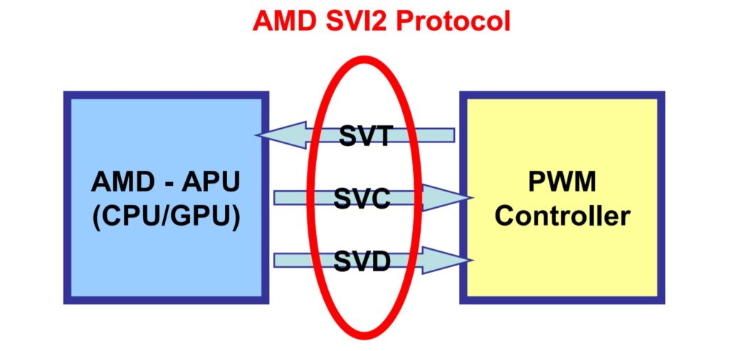
In systems using VRMs, the needed supply voltage is communicated by the MCU to the VRM at startup via a number of bits called VID. The VRM initially provides a standard supply voltage to the VID logic, which is the part of the processor whose only aim is to then send the VID to the VRM. When the VRM has received the VID identifying the required supply voltage, it starts acting as a voltage regulator, providing the required constant voltage supply to the processor. VID enables a single VRM to support multiple CPU/GPU models and enables the processor to communicate with the VRM to reduce power consumption during periods of low activity or when in idle or sleep mode.
VID signals can be from 4- to 8-bits long. Some VRM controllers can accept multiple VID signal bit widths. For example, a 6-bit VID can enable 10mV output voltage step resolution. The number of bits also determines the number of distinct voltages that can be identified; a controller with 5-bit VID would output one of at most 32 distinct output voltages. In many instances, some of the VID commands may be reserved for special functions such as shutting down the unit; hence a 5-bit VID unit may have fewer than 32 output voltage levels.
DVS, AVS, and DVFS
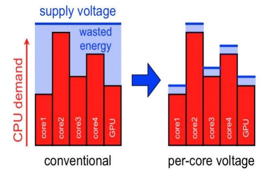
The operating conditions of systems can be highly variable. When powering multi-core CPUs, energy consumption can be substantially reduced if the supply voltage is modulated rapidly based on the instantaneous power needs of individual cores. Three techniques are used to reduce core energy consumption; dynamic voltage scaling (DVS), adaptive voltage scaling (AVS), and dynamic voltage and frequency scaling (DVFS).
DVS power management involves increasing or decreasing the operating voltage of a core based on specific needs. When DVS is used to reduce the operating voltage and conserve energy, it is referred to as undervolting. Undervolting is commonly implemented in laptop and tablet computers to conserve battery power. When DVS is used to increase the operating voltage, it is referred to as overvolting. Overvolting is used to support higher clock frequencies and higher levels of performance. The term “overvolting” is derived from the use of “overclocking” when referring to clocking a CPU at unusually high frequencies.
AVS is similar to DVS in its goal to save energy, but AVS adapts the voltage directly to the conditions on the chip. Where DVS is an open-loop control, AVS is a closed-loop control where there is direct feedback between the performance of the chip and the voltage provided to it. That enables AVS to respond to real-time power needs and chip-to-chip variations and changes in performance as the chip ages.
Clocking a given core more slowly reduces energy consumption. DVFS is an energy-saving method based on:
- The linear relationship between clock frequency and power consumption.
- The quadratic relationship between power consumption and operating voltage. This relationship is P = C × V2 × f. Where: P Is the dynamic power, C is the switching capacitance of the logic circuit or core, V is the operating voltage, and f is the clock frequency.
Reducing the clock frequency reduces energy consumption, and at a lower clock frequency, a core can also operate at a lower voltage. The advantage of DVFS is that it reduces both dynamic and static power consumption. DVFS can also be initiated to keep a core or the overall CPU within thermal limitations.
There is a specific relationship between the core’s operating voltage and the range of frequencies the core can be used safely. A given operating frequency, together with its corresponding operating voltage, is called an Operating Performance Point (OPP). For a given system, the range of attainable OPPs is called the system DVFS curve.
DVFS is implemented by the operating system (OS) to save energy and/or to keep within thermal limits. The OS uses “policies” to manage the power consumption and performance of the system. A policy designed to save energy will use lower clock frequencies resulting in lower performance. A policy designed to maximize performance will use higher clock frequencies and use more energy.
Circuit board parasitics and the relatively slow switching frequencies of discrete VRMs preclude them from being used to implement full DVFS. Discrete VRMs can scale voltage levels only in tens of microseconds (called “coarse-grained DVFS”), too slow to realize the full benefits of DVFS. Realizing the full benefit of DVFS requires the use of FIVRs or IVRs that can support voltage scaling in less than a microsecond. And, while AVS and DVS are done in hardware, DVFS requires software and is controlled by the OS.
GaN-based hybrid VRM for 48V to 1V direct conversion
To support the growing power demands of data centers, 48Vdc power distribution is replacing conventional 12Vdc power distribution. While the move to 48Vdc can reduce distribution losses by 16x, it makes the design of VRMs exceedingly difficult. The large conversion ratio from 48V to core voltages as low as 1V makes it impossible to achieve the desired VRM efficiencies and power densities.
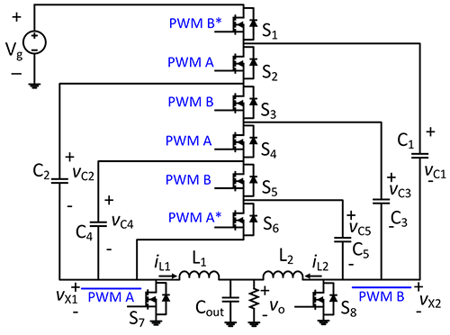
A variation on the Dickson switched-capacitor converter called a Dual Inductor Hybrid Converter (DIHC) has been developed to address the need for 48V-to-1V VRM power conversion. The DIHC eliminates two large synchronous switches and has two interleaved inductors at the output. It uses fewer switches and has more effective switch utilization than the Dickson converter, leading to substantially lower conduction losses and a smaller equivalent output impedance. The DIHC has a peak efficiency greater than 95% and is over 90% efficient at 20% loading. It achieves a power density of 225W/in3.
Summary
VRMs are complex and specialized buck dc/dc converters used to power CPUs and GPUs. They can take the form of discrete components on the motherboard, a separate module that plugs into a dedicated connector on the motherboard, and they can be found integrated directly into the CPU/GPU. More than just powering the CPU/GPU, a VRM enables dynamic and optimal performance that can be tuned for maximum energy savings, maximum computing performance, or an intermediate level of both.
References
A 95%-Efficient 48 V-to-1 V/10 A VRM Hybrid Converter, Efficient Power Conversion
Voltage regulator module, Wikipedia
What is a VRM and Why Does My CPU/GPU Need One?, Cadence Design Systems


Leave a Reply