Recent enhancements to the classic BJT show that the classic transistor has plenty of life left and can challenge SiC and GaN devices in some power applications.
Amidst the advances in CMOS and wide bandgap semiconductor technology, you can easily forget that the first transistor invented by William Shockley in 1949 was a bipolar junction transistor (BJT). Even though they have fallen out of vogue, these humble devices continue to function efficiently and reliably in huge volumes within various types of electronic equipment. Indeed, in some applications, BJTs can outperform their more illustrious CMOS counterparts. Recent enhancements in BJT technology will keep them an important part of the semiconductor technology landscape.
Low saturation voltage
Some inherent disadvantages of BJTs compared to MOSFETs include their requirement for a continuous base current and a higher saturation voltage across the collector-emitter terminals. The high current gain (hFE) and low saturation voltage (VCEsat) of “low VCEsat” BJTs, however, reduce the base current drive and power dissipation, thereby making them a viable alternative to MOSFETs in the following applications.
Load-switch
A common version of the load switch, where the load is ground-connected, and the positive supply voltage is turned on and off, is shown in Figure 1. Reverse currents from the output to the input are blocked by the inherent feature of the BJT. This is an important feature if you use a load switch in a charger application; for example, a battery connected to the output terminal must not feed current into the input power supply when switched off. If the load transistor is a p-channel MOSFET (instead of a BJT), the body diode could conduct a reverse current to prevent this from happening. You would need an extra diode or a second FET, which adds additional cost. Because the diode’s forward voltage adds to the FET’s RDSon losses, the efficiency of this type of load switch is reduced.
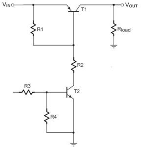
Another advantage of using a BJT is that it only requires a small control voltage. BJT’s base-emitter diode forward voltage is approximately 0.7 V with only a small spread. On the other hand, the gate-source threshold of a MOSFET can have a wider spread of values. That means you need a larger control voltage.
To be fully turned on, a MOSFET must also apply a higher drive voltage than the gate-source threshold. If you need to switch small voltages, then a p-channel MOSFET could create issues in the load path. Yet another advantage of using a low VCEsat BJT in this application is its superior ESD robustness.
Low-voltage dropout regulator
Within the family of linear regulators exists a subgroup called low-voltage dropout regulators (LDOs). While standard linear regulators based on an NPN BJT require headroom between their input and output voltage of at least VCEsat + VBE, the only headroom required by an LDO realized with a PNP BJT is VCEsat. Using a low VCEsat BJT helps to keep this headroom very small. Figure 2 (a) shows an LDO using an NPN BJT in the load path, while Figure 2 (b) uses a PNP BJT. These linear regulators are optimal for battery-powered applications because of their high efficiency. The high forward gain of low VCEsat BJTs increases efficiency because they need low driving currents.

Device matching is still relevant
In many electronic circuits, the exact values of BJT device parameters are not especially important if they lie within a specified range. Many applications, however, require BJTs whose parameters closely match each other. While many semiconductor manufacturers offer individual BJTs whose parameters have tight tolerances, these may still not provide the necessary level of matching, especially as the operating temperature of an application increases. You may, therefore, need matched pairs.
Current mirror for biasing
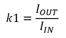
Like that shown in Figure 3, the current mirror circuit is commonly used as a current source to ‘bias’ (set the operating point) other application circuits like amplifiers or comparators. Assuming that both transistors are identical and R1 = R2, IOUT will exactly replicate IIN. This is expressed mathematically as:
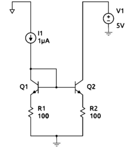
For a perfectly matched pair, the ratio between the selected values for R1 and R2 sets the value of k1. IOUT should also track IIN across the input current values required by design. However, slight differences in the physical characteristics of the BJTs can cause an unwanted deviation, thereby making it more difficult to precisely define the behavior of the application that the mirror circuit is biasing.
Current sensing
Newer applications such as electric vehicles (EVs) or mild-hybrid vehicles (HEVs) require that load current drawn from a battery be sensed close to the battery. The sensing current must be converted to a voltage within the input range of an analog-to-digital converter (ADC) or a microcontroller (MCU). Thus, it must be small, and the voltage must be provided relative to the ground. This can be done using a current sensing circuit, as shown in Figure 4, where V1 represents the 48 V battery voltage and I1 is the load current drawn from it. This circuit is based on two current mirrors – one pair of NPN BJTs and another pair of PNPs. A load connects to the battery through a 50 mΩ current-sensing resistor. For a maximum load current of 10 A, the input voltage to the sensing circuit will be 0.5 V. The BJTs in each current mirror pair should be as closely matched as possible to prevent offsets in the output voltage. You may need trimming to ensure the voltage stays within the ADC’s input range to achieve that match.
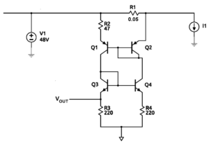
For each of these applications, you should use dual BJTs, which are two dies assembled in a single package. The proximity of the two dies ensures that their temperature will be tracked almost identically. Furthermore, using matched devices harvested from the same wafer area minimizes the possibility of deviations in the manufacturing process that could cause major differences in electrical parameters. This means their parameters have almost identical values, ensuring almost perfectly symmetrical behavior. Matched pair transistors eliminate the requirement for costly trimming in current mirror and differential amplifier applications, and compared to standard double transistors, they ensure accurate base-emitter voltage and current gain matching and are also fully internally isolated.
Voltage and current sources
Stable voltage or current sources are key requirements for most electronic applications, and while many integrated solutions offer these functions, they can be expensive. Thankfully, you can still implement these functions quickly and inexpensively using discrete BJTs.
Voltage regulation
Switching regulators are widely used as power supplies, but linear regulation is still needed for applications to reduce electromagnetic interference (EMI) and voltage ripple. For example, when powering application-specific chips (ASICs), microcontrollers (MCU), application processors, and sensors. This is why linear regulators are often included after switching regulators in power supply blocks. Unlike switching regulators, the difference between input and output power is dissipated in a pass transistor such as a BJT, as shown in Figure 5. To minimize these power losses, linear regulators are mainly used in applications where the difference between input and output voltage is small or only small output currents are required. Figure 5 shows a basic linear regulator with feedback regulation where a PNP BJT drives the NPN pass transistor.
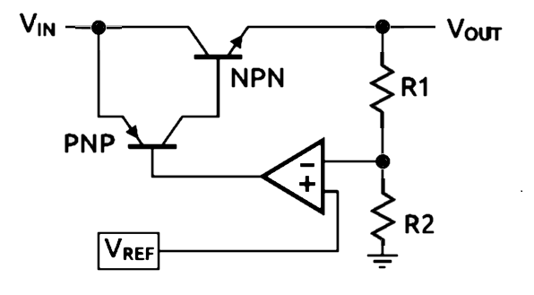
The minimum voltage drop across the BJT output stage is the sum of the emitter-collector saturation voltage of the PNP transistor and the voltage drop of the base-emitter junction of the NPN:
An error amplifier tracks output voltage using a resistor divider to regulate it. The error amplifier compares this feedback voltage to a reference voltage (VREF) and adjusts the PNP-BJT base drive accordingly, which in turn adjusts the drive of the pass transistor. In this way, if the feedback voltage exceeds the reference voltage, the error amplifier lowers the base current and vice versa.
Current stabilization
Loads such as an LED string can’t be directly connected to a constant voltage source — they require a stable current. This scenario arises because an LED’s forward voltage is temperature-dependent with a negative thermal coefficient. Thus, the current would continuously increase due to self-heating and/or increasing ambient temperature. This could eventually lead to thermal runaway, potentially destroying the LEDs in the string. Figure 6 shows how to implement a simple current sink using an NPN or a current source using a PNP BJT:
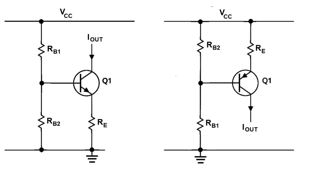
Here, the output current is given by:
Unfortunately, the stability of the output current is impacted by the negative temperature coefficient of VBE, which is approximately −2 mV/K, meaning the change in output current over temperature is:
You can partially compensate for this by using a PN or Zener diode to replace the ground-connected resistor in the base bias circuit. The benefit of using a Zener diode is that IOUT is independent of VCC, increasing its immunity to supply voltage ripple. Very precise current stabilization can be achieved by combining a BJT with a base drive controller (shunt regulator) to provide an accurate and thermally compensated control loop.
Extra insight through thermal models
Predicting the thermal behavior of discrete BJTs and their packaging is critical for some applications, and this is possible using Foster and Cauer RC models for thermal impedance.
The Foster model
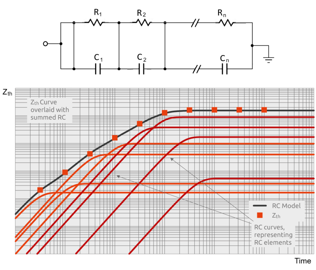
The Foster thermal model of a BJT is derived by semi-empirically fitting a curve to Zth, resulting in the one-dimensional RC network shown in Figure 7. Note that a Foster model’s R and C values don’t correlate with actual locations on a physical device. The model parameters Ri and Ci are the thermal resistance and capacitance values used to create the thermal model for calculating the thermal impedance of a device. Manufacturers often provide thermal models for their BJTs that you can use to verify device behavior using software simulation tools.
The Cauer model
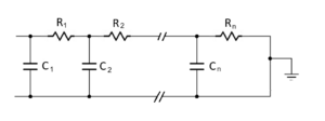
The RC network also represents a Cauer model, but unlike the Foster model, thermal capacitances are connected to thermal ground (ambient temperature location) as shown in Figure 8, and they also have physical meaning, which allows them to be used in determining the temperature of internal layers within a semiconductor structure. An advantage of using the Cauer model is that it will enable the addition of external components to the device model, such as the thermal models for PCBs, heatsinks, etc., which is impossible using a Foster model.
Conclusion
While CMOS and wide bandgap semiconductor technologies have stolen the limelight, bipolar junction transistors remain unsung heroes in many electronic applications. They even outperform their more illustrious counterparts in some key applications. This article reviewed some of these use cases. It showed how advances in BJT technology ensure that these versatile devices are unlikely to disappear from the electronic landscape anytime soon.
Related EE World articles
When to use NPN and PNP transistors and FETs
What’s the difference between an IGBT and an IGCT?
Not to be forgotten: the simple, bipolar SCRs and TRIACs
Biasing bipolar transistor circuits
Dispelling Myths: Don’t believe it when they say you need a bipolar gate drive for eGaN FETs
FAQ on pull-up/pull-down resistors, Part 1






There are many good reasons, these are not the best. We still use RF BJT’s in some of our products for their very low capacitance and high bandwidth.
Also BJT’s can be paralleled in linear operation, MOSFET’s and GaN FET’s can’t.
In most, but NOT ALL cases, WBG wins