Bipolar transistors used in linear applications need “biasing”, as do other transistors (JFET, MOSFET) when used for linear applications rather than as switches. When used as a “switch” you simply want the transistor to be ON or OFF and don’t really care about having in-between states, although when you are switching high power or switching quickly the in-between states become important. Also, if you are designing a high speed switch then biasing actually may come into the design to speed up the switching and minimise transition times. For a linear amplifier, the standard common emitter amplifier is a typical example and there are plenty of very good tutorials to explain how to design one on the internet – simply search for biasing common emitter amplifiers and you will find many good examples.
Biasing is about choosing the voltages at various key points in a circuit and the currents flowing through devices to meet the design objective. In the case of a common emitter amplifier you will have a signal source impedance which dictates what your amplifier input impedance should be to minimise loading of the signal source. You will have a gain and bandwidth requirement and a load impedance to drive. Lastly you will also have a voltage swing to consider. In the end you will have a circuit where you have chosen all the voltages and currents to meet the design objective:
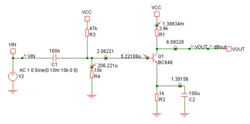
So, in this circuit (which has a 12V supply) you can see the voltages at the important points as well as the currents in the various devices. The tutorials on the internet will help you choose all the values to meet your requirements. Choosing each component value is important if you care about the performance and meeting a specification.
But what about other amplifier designs? The common base amplifier for example looks a little weird depending on how it is drawn, and it’s purpose is not obvious when you learn it has a low input impedance and high output impedance:
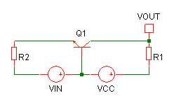
While common base amplifiers are sometimes used like that in radio frequency (RF) amplifiers, if you redraw it in a more common circuit – the cascode amplifier – it makes more sense.
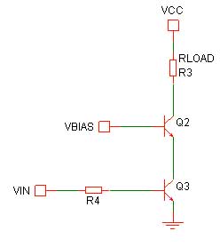
Here, Q2 is actually the common base amplifier. Its base is at a fixed voltage which will be chosen to ensure Q3 doesn’t saturate and it simply allows Q3 collector to be almost at a fixed voltage and Q2 passes Q3 collector current to the load. This improves the speed by isolating the effect of Miller capacitance. This has been covered in more detail in my earlier blog on cascode amplifiers.
Another place where the common base amplifier sneaks in unnoticed is in the “long tailed pair” or differential amplifier.
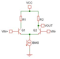
One of the ways you can view this circuit is as an emitter follower, Q1, driving a common base amplifier Q2 which may seem counterintuitive to its symmetry. However, it can be analyzed in that way. IBIAS can be simply a resistor. The transistor bases must be far enough above the ground to ensure the base-emitter voltage does not drop below the nominal 0.7V required for the transistor to be conducting and the collector resistors must be chosen to ensure that the transistors do not saturate. If IBIAS is replaced by a resistor then you need to ensure that the transistor emitter voltage does not drop too low as the bias current will drop as the emitter voltage drops.
Biasing becomes more complicated when you are designing a double balanced mixer, either discrete or using the MC1496:
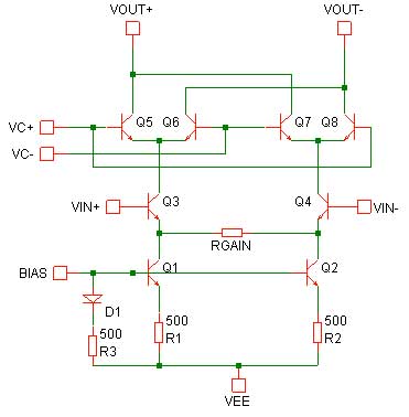
Here, the BIAS input is used to set the bias current in the two arms of the mixer. There will be external resistors on the two outputs so the bias current will set the nominal output collector voltage. The inputs need to be biased to ensure Q3/Q4 emitters do not drop too low and cause Q1/Q2 to saturate when the voltage on Q1/Q2 emitters is taken in to account, but not so high that you then reduce the headroom for the next transistors upwards in the chain – Q5/6/7/8. The carrier inputs, VC, need to be similarly biased to ensure Q5/6/7/8 emitters don’t cause Q3/Q4 to saturate. The voltage swing of each input needs to be taken into account when setting the bias points although a double balanced mixer will usually have significant gain so the input swings will be small compared to the output swing. The carrier voltage input swing can be high though.
In each case of biasing you are often breaking your supply voltage into a series of steps and trying to ensure that no transistors saturate at any point, even with a large signal present, while trying to ensure enough voltage left for the output signal which will usually have a larger swing than the input signal. So, in the double balanced mixer on a 5V supply you might set BIAS at 1.2V, VIN at 2V, VC at 3V and the output at 4V. With a low voltage supply there is not a lot of room to squeeze in all the voltage drops required. Ideally you would keep the base-collector junctions reverse biased for speed so you don’t want the transistor collectors dropping below their base voltage. The 0.7V base-emitter voltage of a transistor takes quite a chunk out of your total supply when you have three devices in series and would make a 3V design tricky. The same problem occurs when design analog CMOS ICs where there isn’t room for cascode loads with a low voltage supply which is why folded cascode configurations are often used – but that subject will be saved for another time.


[…] difference between an IGBT and an IGCT? Not to be forgotten: the simple, bipolar SCRs and TRIACs Biasing bipolar transistor circuits Dispelling Myths: Don’t believe it when they say you need a bipolar gate drive for eGaN FETs FAQ […]