By Peter Friedrichs, Infineon Technologies
SiC and GaN devices operate at higher stress levels than silicon devices. The semiconductor and automotive industries have strict qualification tests for that.
Silicon carbide (SiC) and gallium nitride (GaN) wide bandgap (WBG) technologies are well known for their performance advantages over silicon (Si) in many high-power areas, including their high efficiency and high switching frequencies. Unlike single-crystalline silicon, however, SiC and GaN have unique design and application issues that engineers need to address when qualifying these technologies for designs.
Unique aspects of SiC and GaN compared to Si
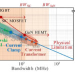
SiC and GaN WBG power devices are used in power conversion, switching, and control applications, so potential aging is part of the critical design decisions. This is especially important in more demanding automotive and industrial applications, but system designers in data centers, consumer, commercial, and other products should be equally knowledgeable about these issues. Figure 1 shows the extended operating range of SiC MOSFETs and GaN high electron mobility transistor (HEMT) technologies.
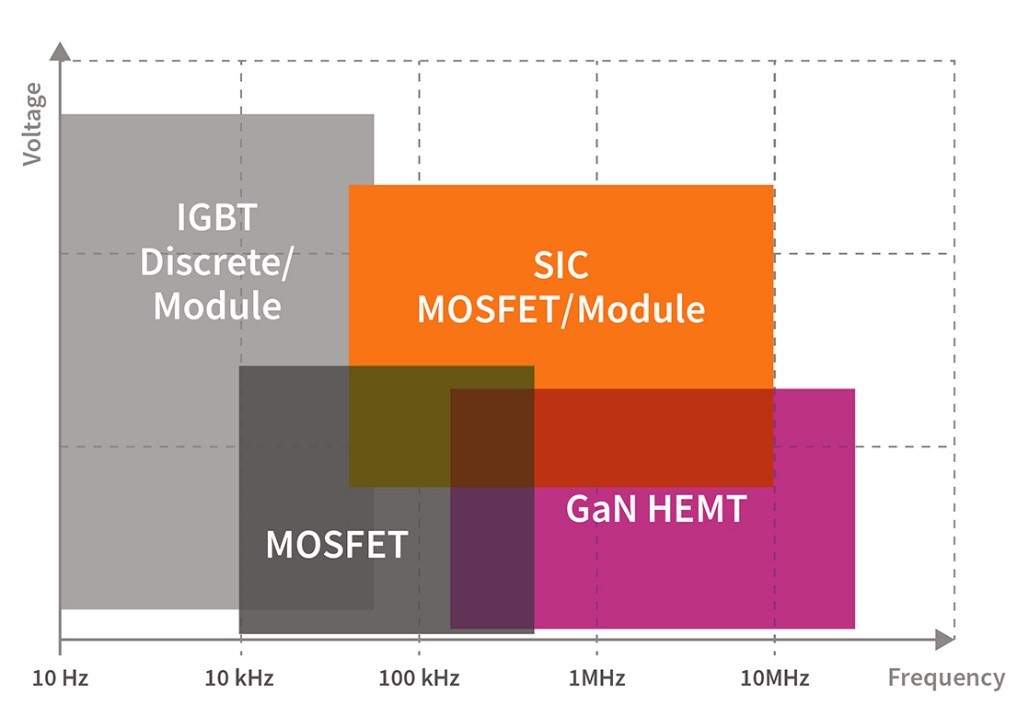
SiC MOSFETs extend the voltage and switching frequency beyond Si devices. While not as high voltages, GaN extends the frequencies into a considerably higher range. To address the extended operating ranges in Figure 1, Figure 2 compares the key parameters of SiC and GaN technologies to Si.
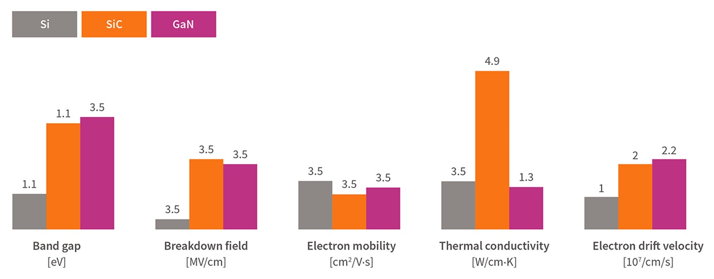
Unlike Si, SiC has much higher thermal conductivity and breakdown electric field strength (correlated to the wider band gap). These factors make it an excellent material for high-frequency and high-power applications. All these higher-stress situations require qualification testing to provide proper long-term functionality and acceptable service life. One of the critical differences between SiC and Si-based MOSFETs occurs due to extrinsic defects — tiny distortions in the gate-oxide, which behave like a local oxide thinning. While a thicker gate oxide process and related screening procedures minimize this issue, other factors and differences in design and applications must also be addressed.
Likewise, GaN has some behaviors that differ from those of Si devices. One example is dynamic RDS(ON), an increased resistance that can occur over time. You must also consider the differences between Si and GaN device structures and material systems when developing a qualification plan for GaN HEMTs.
Industry testing standards and reliability
The Joint Electron Device Engineering Council (JEDEC) and Automotive Electronics Council (AEC) are two industry organizations that provide specific and detailed specifications for testing and qualifying semiconductor devices. Both organizations focus on reliability issues and the expected life of power semiconductors.
To address aging and reliability requirements in automotive applications, the Automotive Electronics Council created AEC-Q101 (Stress Test Qualification for Automotive Grade Discrete Semiconductors) applicable to Si. It will be adapted to SiC and GaN power devices. With the higher voltages in electric vehicles and increased life expectancy, modifications are being proposed for these WBG devices.
Addressing a wide range of components, JEDEC has JESD47 (Stress-Test-Driven Qualification of Integrated Circuits) that provides a baseline qualification approach for less extreme applications. JEDEC subcommittee JC-70.1 delivers tests, datasheets, and qualification standards unique to GaN, subcommittee JC-70.2 for SiC technologies. JEDEC developed several guidelines and test methods for GaN and SiC devices in this course. This includes JEP173 Dynamic On-Resistance Test Method Guidelines for GaN HEMT-Based Power Conversion Devices. To ensure that industry efforts adequately address the lifetime and aging idiosyncrasies of SiC and GaN power devices, Infineon has initiated and contributed to establishing both JEDEC subcommittees JC-70.1 and JCX-70.2.
Tests and criteria
Two important reliability issues for SiC power devices are gate-oxide and threshold-voltage stability. Because SiC power MOSFETs include gate-oxide layers, a process called time-dependent dielectric breakdown (TDDB) occurs over time. The gate oxide breaks down, deteriorates, and fails after exceeding its intrinsic life.
Another effect in SiC power devices and Si technology is bias temperature instability (BTI). With a constant DC bias applied to the gate of a SiC (or Si) MOSFET at elevated temperatures, threshold voltage and potential on-resistance may shift. The amplitude and polarity of the shift depend on the stress conditions (bias, time, and temperature).
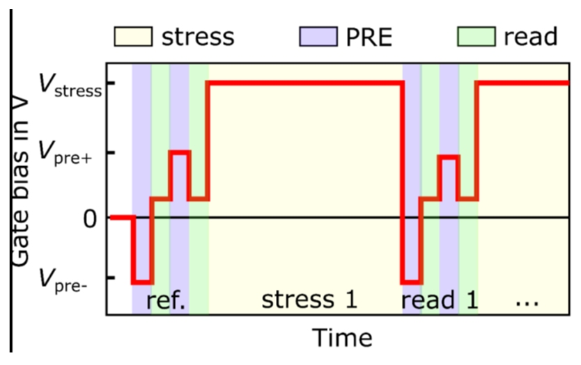
Si technology qualification has used a measure-stress-measure (MSM) sequence consisting of a repeated applied gate bias and temperature stress followed by a readout to qualify a design. However, the readout timing significantly impacts the threshold voltage drift measurement.
Infineon has proposed a positive BTI (PBTI) test sequence for more excellent repeatability, as shown in Figure 3. The preconditioning pulses more closely represent the gate switching in the application and reduce the influence of readout delays and device history. Since DC BTI in SiC can cause reliability concerns, it needs to be minimized by optimizing device processing and carefully assessing using appropriate measurement methods. This test facilitates that process.
To increase the probability of finding extrinsic failures in SiC, Infineon developed the marathon stress test as a baseline for effective screening procedures. Performed at a much lower gate bias than a TDDB test, the marathon test’s goal is to detect early device failures caused by critical extrinsic gate-oxide distortions and extract important model parameters to design test patterns for the outgoing product test. The tests use stress periods of 100 days. Thousands of devices are stretched parallel in a parameter range close to operating conditions.
Other mandatory qualification tests for the release of any technology include High-Temperature Reverse Bias (HTRB), High Humidity, High Temperature and High Voltage Reverse Bias test (H3TRB), and High-Temperature Gate Stress (HTGS) tests. For a standard H3TRB qualification, T = 85°C, the relative humidity (rH) = 85% and VDS = 80V. However, with operation at much higher voltages, HV-H3TRB with VDS = 80% VDSS is a more appropriate measure to test the reliability of a SiC device against humidity. Table 1 shows this and other modified test conditions for automotive qualification at Infineon.

GaN tests
The difference between silicon and GaN HEMT devices is that when tested at accelerated drain-to-source voltage and temperature conditions, GaN HEMTs exhibit a failure rate that depends strongly on voltage. It is important to quantify, and model GaN HEMT reverse bias lifetime to ensure operation to designed limits. GaN devices do not avalanche and can withstand voltage stresses much higher than their silicon counterparts without failure. However, their lifespan at such high voltages is limited.
A second key new degradation mechanism for GaN devices is the safe operating area (SOA) switching or dynamic high-temperature operating life (DHTOL). To address this mechanism, Infineon and other semiconductor manufacturers publish long-term application switching data showing stable device operation in hard-switching applications for 1,000 hours to 3,000 hours.
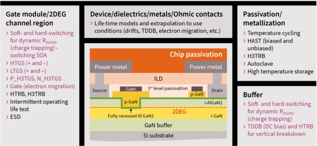
In GaN devices, the effect of dynamic RDS(ON) is caused by charges trapped during processing or due to the dynamic impacts that can interact with and modify the two-dimensional electron gas (2DEG) density in the channel, increasing RDS(ON). During development, it is important to ensure that the related increase in conduction losses is low during typical applications and that dynamic RDS(ON) does not fail. Figure 4 shows a summary of GaN-specific tests for aging and more. Passing these tests has qualified GaN devices and minimized aging effects.
Aging from a semiconductor technology perspective
Attention to detail allows fine wines and power semiconductors to age well and achieve their objectives. Because they operate at higher stress levels from higher operating frequencies and/or higher operating voltages than Si and have considerably different materials in their designs, SiC and GaN WBG devices require evaluation and qualification to much stricter tests. Ongoing R&D is improving the impressive reliability capabilities of the newest SiC and GaN WBG power transistors. As each generation of devices advances, aging aspects will also improve.
References
How Infineon controls and assures the reliability of SiC-based power semiconductors
Reliability and qualification of high-voltage CoolGaN™ GIT HEMTs



Leave a Reply