By Didier Balocco, onsemi
The trend towards higher voltages opens new opportunities for design with Silicon Carbide.
With its higher electron mobility, lower losses, and ability to work at higher temperatures, the case for silicon carbide (SiC) devices in challenging power applications is widely accepted. While the benefits of silicon are significant in key applications, further advancement is required, especially to reduce size and cost while improving efficiency.
In the automotive and renewable sectors, there is a trend towards increasing voltages to meet these goals. However, to achieve this, SiC devices capable of operating at these voltages must be freely available.
The move to higher voltages to increase efficiency has its foundations in the most fundamental law in physics, Ohm’s Law. This tells us that losses increase with the square of current; therefore, reducing current will significantly improve efficiency. Ohm’s Law also tells us that, for the same power, we have to double the voltage if we want to halve current.
In halving the current, the static losses due to conduction losses in semiconductors and cabling are reduced by a factor of four. It is for this exact reason that electricity grids operate at extremely high voltage levels.
While it might seem evident that industrial and automotive applications move to extremely high voltages, this is impractical due to the availability of components supporting such voltages.
Power device switching
In a switching power converter, a power device has three roles: blocking, conducting, and switching between the previous roles. As voltage increases, the challenge is with the blocking aspect, as high voltages will appear across the device, and without the appropriate construction and materials, a catastrophic failure could occur.
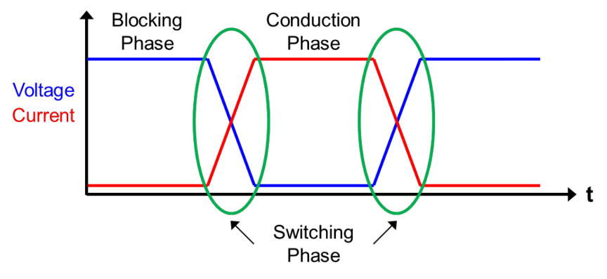
Therefore, SiC devices with higher blocking voltages across their drain and source pins (VDS) will be required to access the efficiency benefits of higher voltage operation. Currently, many devices with 650 V capability and 1200 V-rated devices are becoming more common. However, higher voltage-rated devices will be required to address these higher voltages, with an appropriate design margin to ensure reliability.
Applications moving to higher voltage operation
Greater efficiency will benefit applications operating at higher power levels significantly. In the renewable field, both wind and solar power generation are moving to higher voltages. With solar photovoltaic (PV) systems, the DC bus voltage from the PV panels has increased from 600 V to 1500 V to enhance efficiency.
Greater efficiency here simply means that more natural solar or wind energy is available to be used immediately or stored for later use. While both forms of energy may appear to have infinite capacity, they are both subject to the vagaries of weather, which can limit output.
Also, if the system is more efficient, it will be smaller and lighter, which is a significant benefit for roof-mounted installations.

One of the reasons often cited for slower-than-expected growth in EVs is the time taken to charge and the limited battery range. To address this, automakers are replacing 400V battery strings with 800V versions. Charging speed is determined by the charger’s output power, which is limited by the system voltage and output current. While increasing the current reduces charging times, it also increases the heat generated and system energy loss, reducing the charger’s efficiency and elevating the cooling demands. Alternatively, the EV charger’s power output is significantly increased by increasing the voltage and maintaining a similar current level. This lowers the vehicle’s charging time without substantially raising the thermal considerations or reducing system efficiency.
The reduced current and enhanced efficiency will reduce the on-board charger’s size, cost, and weight (OBC) as thinner cables can be used and less heatsinking is required. As the OBC remains on the vehicle, any weight reduction will increase the vehicle’s range.
Looking to the future, as electric propulsion moves into commercial vehicles, the batteries will be significantly larger, and more power will need to be transferred efficiently to charge in a reasonable time. As a guide, the Megawatt Charging System (MCS) is rated for a charge rate of 3.75MW – 3,000A @ 1,250 VDC.
SiC breakdown voltages
One of the challenges in developing semiconductor power devices in vertical structures with higher breakdown voltages is that there is a corresponding increase in conduction losses due to the increase in RDS(ON). The drift layer is generally thicker in devices with higher withstand voltages, which increases conduction losses.
So, while there are efficiency benefits to increasing operating voltage, the corresponding increase in conduction losses within the MOSFET will negate some or all of these benefits.
SiC-based power devices, however, can offer higher breakdown voltages with a substantially thinner drift layer than the equivalent silicon device, resulting in lower forward voltage drop and reduced conduction losses.
A modern, high-breakdown SiC MOSFET
With the need for MOSFET devices with breakdown voltages in excess of the operating voltage, onsemi has developed a range of new SiC MOSFETs specifically for such applications.
onsemi’s NTBG028N170M1 is an N-channel planar EliteSiC MOSFET that is optimized for fast switching applications at high voltages with a VDSS of 1700 V and an extended VGS of -15/+25 V. The device can support drain currents (ID) up to 71 A continuously and 195 A when pulsed.
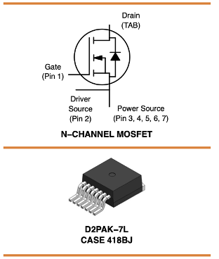
The robust device mitigates conduction losses with an excellent RDS(ON) value of just 28 mΩ (typ.), while an ultra-low gate charge (QG(tot)) of just 222 nC ensures low losses during high-frequency operation. The device is housed in a surface mountable D2PAK–7L package, which reduces parasitic effects during operation.
Supporting the MOSFETs, onsemi offers a range of 1700 V-rated SiC Schottky diodes that enhance the voltage margin between VRRM and the peak repetitive reverse voltage of the diode. In challenging applications, the 1700 V diodes will deliver lower VFM, maximum breakdown voltage, and excellent reverse leakage current even at high temperatures, thereby equipping design engineers to achieve stable high voltage operation at elevated temperatures.
Summary
In every area of power electronics, efficiency is a primary goal. Not only does it reduce operating costs, but it also allows designs to be smaller, lighter and lower cost. With highly efficient semiconductors already commonplace, designers are looking to other areas of the system to deliver more efficiency.
Increasing the system voltage reduces the current and has a significant impact on reducing losses. However, this has proved challenging until now, as increasing the breakdown voltage of MOSFETs has also increased their conduction losses.





Leave a Reply