Silicon Carbide FETs go beyond silicon to extend reach to high pulse currents in power conversion applications.
Wide bandgap (WBG) semiconductor devices, such as Silicon Carbide (SiC) field-effect transistors (FETs), are renowned for their minimal static and dynamic losses. Beyond these attributes, this technology can endure high pulse currents, proving particularly advantageous in applications like solid-state circuit breakers. This article delves into the characteristics of SiC FETs, offering a comparative analysis against traditional silicon solutions.
The ongoing pursuit to minimize power losses in semiconductor switches is spearheaded by WBG devices, with SiC FETs taking center stage. These devices, constructed as cascodes of a SiC junction-gate field-effect transistor (JFET) and co-packaged silicon metal-oxide-semiconductor field-effect transistor (MOSFET), stand out as normally off devices with user-friendly gate drives. Their impressive portfolio of “figures of merit” outshines competing technologies, specifically focusing on on-resistance per unit die area (RDSxA), a metric capturing the combination of low static and dynamic power losses with cost-effectiveness. Despite their smaller die size, which translates to more units per wafer and reduced device capacitances, SiC FETs defy expectations by exhibiting enhanced temperature tolerance and increased peak current capability. Let’s take a look at the numbers.
SiC FETs On-Resistance performance
Quantifying the performance of a SiC FET, exemplified by the 750V-rated device from Qorvo (part UJ4SC075005L8S in a TOLL package), reveals an RDSxA figure 2.2 times better than Gen 4 SiC MOSFETs, consistently maintained across the entire temperature range. In practical terms, this device displays an on-resistance of 5.4 mΩ at 25 °C and 9.2 mΩ at 125 °C, surpassing silicon or SiC-MOSFETs and Gallium Nitride high-electron-mobility transistor (GaN HEMT) rated at 600/650 V in the same package by a factor of 4 to 10.
To leverage this ultra-low resistance for a high current rating, the sample SiC FET uses silver sinter die attach and advanced wafer-thinning techniques to achieve 0.1 °C/W thermal resistance from junction to case. Additionally, the maximum junction temperature for the SiC device is 175 °C, meaning a single device can continuously handle 80 A when attached to a simple 0.58 °C/W heatsink, with the junction at 175 °C in an 85 °C ambient setting.
SiC FETs peak current rating
The maximum junction temperature (TJ,Max) figure for a SiC device and its current rating are essentially dictated by the packaging used. Despite the intrinsic material capability of SiC to operate safely at temperatures exceeding 500 °C, the maximum is limited to 175 °C in the JFET of a cascode SiC FET. This restriction still allows SiC FETs to handle transient peak currents significantly higher than their continuous rating when initiated from lower temperatures. The transient thermal impedance plot for a specific die and package, such as the aforementioned SiC FET device, outlines these characteristics, as shown in Figure 1.
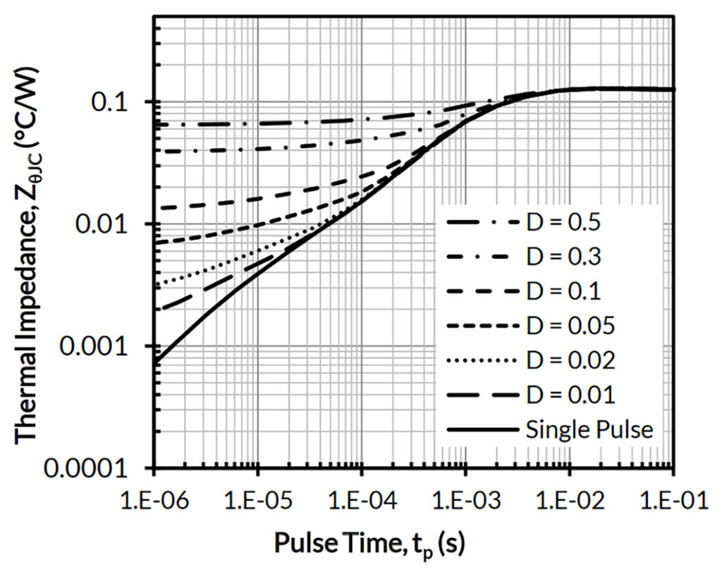
For instance, a single 100 µs pulse results in a transient increase in the junction temperature of about 0.015 °C per Watt of power dissipated. At approximately 10 ms pulse duration, the thermal impedance from junction to case approaches the steady-state value.
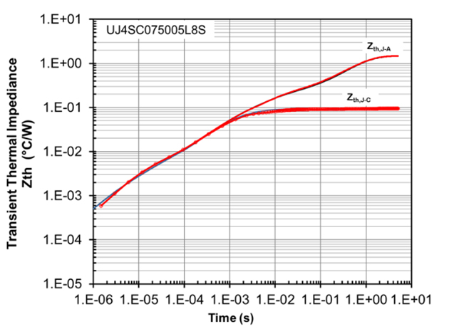
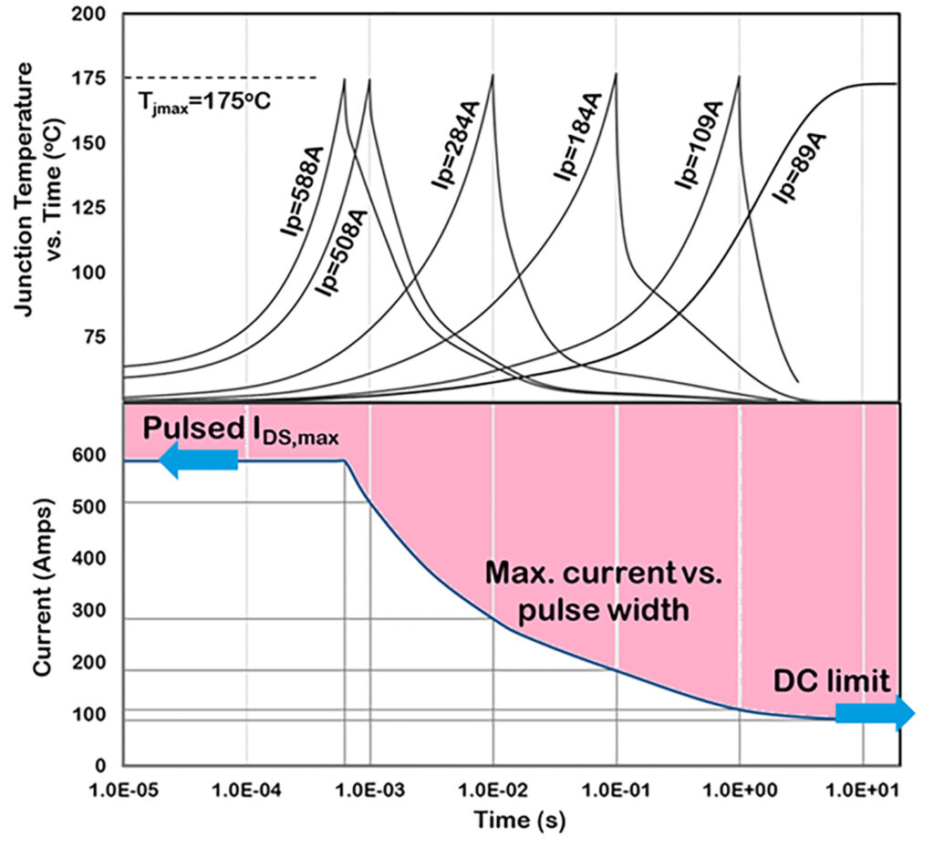
Practical implications for the sample SiC FET device are depicted in Figure 2 and Figure 3. In each scenario, the device case is soldered to a copper plane on a PCB with copper thermal vias through to a back-side aluminum heatsink held at 50 °C, separated by an insulating thermal interface material (TIM). Figure 2 illustrates that a thermal resistance of >1.2oC/W from junction to ambient may be expected, while the die and TOLL package determine the transient thermal response below approximately 1 ms. As depicted in Figure 3, with this arrangement, the continuous rating is 89 A, while the device can handle up to 588 A peak current for a 500 µs single pulse before reaching TJ,Max of 175 °C.
SiC FETs vs. Si-MOSFETs
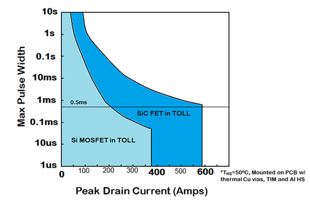
While SiC FETs showcase impressive results, a crucial question arises: how do they compare to Si-MOSFETs, commonly used in lower-power solid-state circuit breakers? The current squared through time (I2t) rating, a familiar measure for devices handling surge current, provides a compelling comparison. The sample SiC FETwithstands 588 A for 500 µs, while the Si-MOSFET rating stands at about 200 A, showcasing an ‘I2t’ difference of 8.6 times, as illustrated in Figure 4.
Additional benefits of high peak current rating
Beyond the evident safety margin provided by SiC FETs under overload conditions, there are further advantages. SiC FETs prove highly suitable for power conversion circuits with inductive loads, where voltage overshoot is expected. These devices exhibit robust avalanche capability and a 750V rating. Moreover, board-mounted DC-DC converters in servers and similar applications increasingly require a high peak power rating in a compact form factor, driven by data-intensive applications such as artificial intelligence (AI), machine learning (ML), and streaming.
Designs of these converters often assume that junction temperatures will approach their maximums due to peak currents experienced. Digital control, facilitated by sensors and prediction algorithms through PMBus™, provides junction temperature feedback, instructing the load to throttle back” as needed to prevent the switch junctions from exceeding their absolute maximum. The ample margin provided by SiC FETs instills confidence in the reliability and lifetime of the power system, potentially reducing the need for multiple paralleled devices and resulting in cost and board area savings.
Solid-state circuit breakers, designed to respond to high fault currents, can use SiC FETs and JFETs for their low voltage drop, displacing insulated-gate bipolar transistors (IGBTs), especially at lower current levels. The peak current rating of SiC FETs adds robustness to these breakers, allowing over-current detection circuitry to incorporate a longer delay before reacting. This attribute makes the circuit breaker more immune to ‘nuisance’ triggering.
Conclusion
Compact SiC FETs with peak current ratings in the hundreds of amps emerge as ideal components for modern power conversion applications demanding high power density and peak load handling. Metrics affirm that these components outperform GaN and Si- or SiC-MOSFET parts in the same voltage class.
This article is part of our 2024 Power Electronics Handbook.




Leave a Reply