
A varactor diode or varicap diode is a semiconductor diode that changes its junction capacitance significantly depending on the applied reverse bias voltage. Many semiconductor PN junction diodes are designed to exhibit specific electrical properties; the varactor diode or varicap diode is one such semiconductor specifically designed to exhibit unique junction capacitance characteristics. These types of diodes are useful in RF circuits for tuning signals; that is why a class of varactor diodes is also called Tuner diodes.
It should be noted that the desired operation of the varactor diode is achieved only in reverse bias condition, but why (we will answer this later in the article)? In reverse bias condition, the internal capacitance of the diode changes significantly with respect to applied reverse voltage. That is why it is not the voltage-current but the voltage-capacitance that is the most important characteristic of a varactor diode.
What is a varactor diode or varicap diode?
A varactor diode is a semiconductor diode whose internal capacitance changes with respect to applied reverse voltage. It is a voltage-controlled device that acts as a variable semiconductor capacitor. It is also called a varicap diode, tuner diode, tuning diode, voltcap, or voltage variable capacitance.
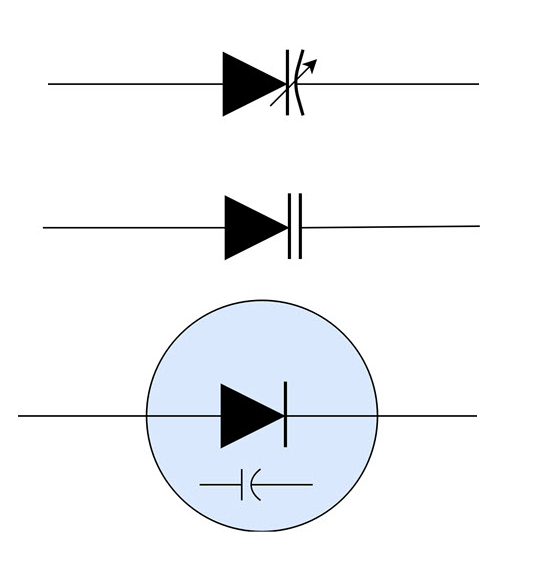
The varactor diodes are shown in electronic circuits by many symbols. The most popular symbols to indicate a varactor diode in a circuit are shown in Figure 2.
Varactor diode construction
Varactor diodes are designed such that they have a very narrow depletion region. Simply a semiconductor diode with p-type and n-type layers. A mesa structure connects The n-type layer to a gold-plated molybdenum stud. This works as the cathode of the diode. A gold wire connects The p-type layer to another gold-plated molybdenum stud. This works as the anode of the diode. Obviously, the polarity of a diode is really important, and that of a varactor diode is even more important as it has to be operated only in reverse bias.
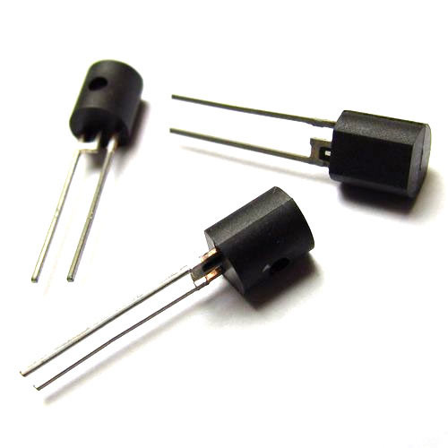
The polarity is often indicated by distinguishing the cathode by a dot or different lead structure or band. The varicap is available in both through-hole and SMD packages. The through-hole packages often have a cathode indicated by a dot or a distinct lead structure. The SMD packages have a cathode indicated by a dot or band at one end. Varactor diodes come in transistor outline (TO), diode outline (DO), small outline diode (SOD), and small outline transistor (SOT) packages. In some packages, three terminals can be seen, of which only two need to be connected. Varactor diodes designed for low-frequency operation are made of silicon, and that designed for high-frequency operation are made of gallium arsenide.
One of the unique things about varactor diodes is their doping. Unlike conventional semiconductor diodes (signal and power diodes), which have uniform doping all across the p-type and n-type layer, in varactor diodes, the concentration of impurity atoms is less near the junction, which gradually increases through the rest of the p-type and n-type layers. This type of doping is done to reduce the length of the depletion region.
How varicap diode works
A varactor diode is expected to work as a variable capacitor. A capacitor is an electrical device that stores charge when voltage is applied across it. As the voltage is reversed, the capacitor discharges the stored charge. When a capacitor charges, current flows through it, building an electrostatic field across it. When a capacitor discharges through a load or during the negative cycle of an AC signal, it lets the current flow in the reverse direction until its plates are electrically neutralized. The capacitance of a capacitor is nothing but a measure of the charge it can store with respect to applied charging voltage. The capacitor can store charge because of the opposition to flow of current through it by its dielectric medium between two conducting surfaces.
A diode has transition and diffusion capacitance. The capacitance is shown by a diode because the depletion region is void of free charge carriers acting as a dielectric medium. The layer of negatively charged ions in the p-type material and the layer of positively charged ions in the n-type material act as conducting surfaces where the charge is stored when no bias or reverse bias voltage is applied.
As mentioned, a varactor diode is designed to have a narrow depletion region. Still, due to the unique doping pattern and physical structure of the diode, the length of the depletion region changes drastically on the application of reverse bias voltage. A capacitor device’s capacitance or charge storage capacity is inversely proportional to the distance between its conducting surfaces and directly proportional to the area of the conducting surfaces. A varactor diode is designed to have a large junction area and narrow depletion region. The mesa structure of the diode at the cathode end and the unique doping pattern achieve this. In unbiased conditions, the diode has the highest capacitance. In the reverse bias condition, as the reverse bias voltage increases, the length of the depletion region increases, and the junction capacitance of the diode decreases. When forward-biased, the depletion region gradually vanishes with the forward voltage, and the diode enters a conduction state. So, to operate a varactor diode as a voltage-controlled variable capacitor, it has to be connected in reverse bias.
Varactor diode characteristics
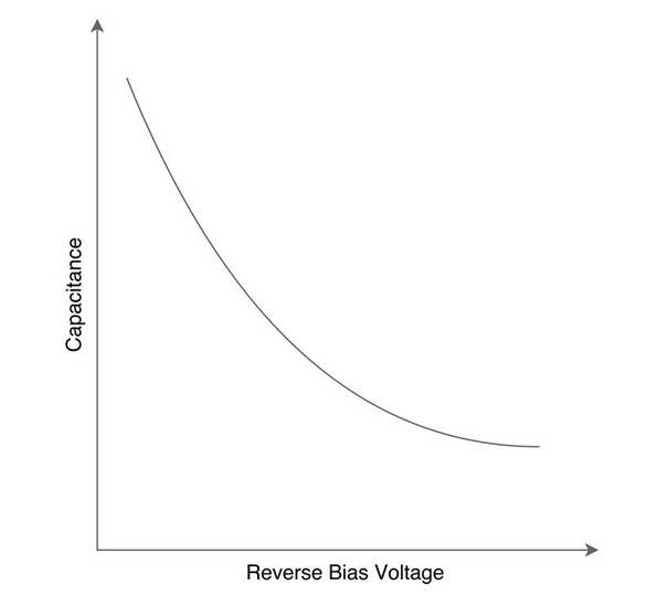
Unlike conventional diodes, which have voltage-current as the most important characteristic, voltage-capacitance is the most important electrical characteristic for varactor diodes. The varicap is designed to have a high range variation of capacitance with respect to applied reverse voltage; Figure 3 is a graph of the typical voltage capacitance of a varactor diode.
Varactor diode types
Varactor diodes are classified as abrupt varactor diodes and hyper-abrupt varactor diodes. In abrupt varactor diodes, the doping is linearly increased from the depletion region to the diode terminals. As a result, the capacitance is almost linearly decreased with a rise in reverse voltage. In hyper-abrupt varactor diodes, the doping is non-linearly increased from the depletion region to the diode terminals. As a result, the capacitance changes exponentially with respect to reverse voltage.
Varactor diode specifications
Some of the important electrical characteristics of a varactor diode include the following:
- Reverse current: this is the reverse leakage current of the varicap through its junction for a specified reverse voltage.
- Capacitance ratio: this is the ratio of minimum capacitance to the maximum capacitance of the varactor diode. A smaller value of this ratio shows an extensive range of capacitance.
- Diode capacitance: this is the minimum capacitance for a specified reverse voltage and AC frequency.
- Junction operating temperature: this is the maximum junction temperature range that the varactor can handle.
- Power dissipation: this is the maximum power dissipated by the diode in its conduction state for a specified ambient temperature. It also indicates the maximum voltage and current the varactor can tolerate.
Advantages of varactor diodes
Several advantages of varactor diodes include being non-mechanical variable capacitors, being easily used within a semiconductor circuit, being small and compact, and producing less noise than other diode types.
Applications of varactor diodes
Varactor diodes are used in tuning circuits or for frequency modulation. Some of the notable applications of varicap are:
- FR filters
- automatic frequency controllers
- high-frequency radios
- bandpass filters
- voltage controlled oscillators
- harmonic generators
- frequency multipliers
Varactor diode reference
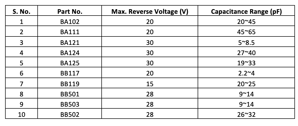
The following table lists some popular varactor diodes with notable specifications:


Leave a Reply