Substituting special capacitors for transformers helps realize ac-to-dc power supplies that are both efficient and compact.
JEFF SORENSEN, HELIX SEMICONDUCTORS
POWER SUPPLIES that convert ac to dc have been a part of nearly every electronics-based product since the popularization of the vacuum tube radio. While the voltage levels have changed, the conversion process has always included a transformer to provide two functions: voltage conversion and safety isolation between the user and the mains power.
For safety, ac-dc conversion circuits must be galvanically isolated from the mains voltages to prevent a shock hazard. Transformers are suited for this purpose because the primary side and secondary side can easily be isolated from each other and the voltage reduced or raised by the transformer’s design. But there are downsides to using transformers – especially when it’s important to improve the power efficiency or reduce the physical size.
Today, capacitors can also isolate circuits from mains power while exhibiting lower inherent losses than transformers. Voltage-level conversion can also take place using high-frequency, switched-capacitor charge pumps, so transformers can also be eliminated for that purpose as well. Thus, capacitors can provide the basic functions that transformers deliver.
It is worth examining transformers and their properties more fully. Transformers have several disadvantages compared to capacitors. First, they are large, usually the largest component in the power supply. They are heavy and add considerably to the overall weight. And they are a major cause of inefficiency in power supply designs.
Transformer losses can be divided into two categories: dc resistive losses in the transformer windings and core losses caused by the magnetic material and physical qualities of the core. I2R power loss arises because of the resistance in the primary and secondary wire. This parameter can be easily calculated knowing the resistance of the wires and the currents they will carry. Though 60-Hz transformers have relatively high dc losses, high-frequency switched-mode transformers can mitigate them somewhat.
The transformer core losses are more complicated and arise from a combination of sources: hysteresis loss, eddy current loss, magnetostriction loss, and leakage inductance.
Hysteresis loss comes from the inherent memory in the core material when it becomes magnetized and, when the field must reverse, “remembers” the previous direction of the magnetic field. It takes energy and therefore power to overcome the residual magnetic field each time it reverses.
Eddy current losses arise from the induced current circulating in the core because the core is also electrically a conductor. Any other conductors or components nearby can have an induced current (noise) from the unshielded magnetic field that surrounds the transformer.
Magnetostriction loss is from grain movement in the core material.
Leakage inductance arises from the imperfect coupling between the primary and secondary inductances of the transformer.
Advantages of capacitive coupling
Capacitors are relatively small compared to transformers and can be made smaller through the careful selection of the values and types used. The higher the operating frequency, the lower the capacitance needed for a given ac impedance (to a point).
Safety capacitors are normally used in products for controlling the conducted and radiated emissions from high-frequency circuitry, and “Y” types are certified by UL and other standards bodies for operation across the isolation barrier. Y1 capacitors are rated for a maximum 500 Vac working voltage and a breakdown voltage of 8 kV. Y2, Y3, and Y4 have progressively lower voltage ratings. Since these capacitors are already intended and approved by UL for use across the isolation barrier, they are also an obvious choice for coupling
the power.
Safety issues such as “touch current” must be considered when using higher-value capacitors across the isolation barrier. “Safety” capacitors are a bit of a misnomer because too much capacitance across the isolation will also allow more ac mains current to pass. Using a high-carrier frequency allows the use of capacitors with smaller values. Also, it is better to use higher voltages, therefore lower current, to keep the reactive impedance losses as low as possible.
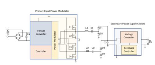
MuxCapacitor is a proprietary charge pump circuit that can either increase or decrease the input-to-output voltage (and current) levels at 99% efficiency. The final chipset will have two separate MuxCapacitor blocks, one on either side of the isolation barrier. To get the best efficiency across the isolation barrier, the voltage on the primary side must be as high as possible. To do this, the primary-side rectified line voltage is regulated to keep the voltage as high as possible before the power is sent across the barrier.
Because the circuit is intended to be used worldwide, this input voltage can vary from 85 to 220 Vac, which after rectification is approximately 120 to 310 Vdc. A primary-side MuxCapacitor stage is used to sense the input voltage and adjust its output to keep the input to the drivers or “modulator” as close to 300 V as possible. It can therefore operate at different levels of gain/attenuation to keep the V+ supply at a constant level.
On the secondary side, the output from the diode bridge demodulator is stored on a capacitor (denoted C3 in the above drawing, Typical transformerless circuit configuration). This is the input to the secondary side MuxCapacitor stage that reduces the voltage on C3 from about 300 to 20 Vdc (nominally) using a variable gain step-down MuxCapacitor. Both the primary and secondary side MuxCapacitor stages can adjust for varying input power and output load conditions.
Referring to the above concept circuit, the modulator operates at approximately 125 kHz. There are two phases to each charging cycle. Mains power is applied to the input of the primary side diode bridge and charges capacitor C4, which connects across the input of the primary side voltage conditioning circuitry. This stage outputs the voltage to supply the V+ to internal switches Q1 and Q3.
For the first phase, Q1 and Q4 are turned on and V+ current flows across the barrier L1/C1. The coupled current then forward-biases diode D1 to charge C3, which connects across the input of the secondary side MuxCapacitor circuitry. The return path of C3’s isolated ground is through D4, then back across C2/L2 and through Q4 to the primary side ground.
After the phase-one charge has been transferred to C3, switches Q1 and Q4 are turned off. The phase-two cycle begins, and switches Q2 and Q3 are turned on. V+ current flows through Q3 across L2/C2 and D3, and again continues charging C3. The return path is now through D2, across C1/L1 to Q2 to the primary side ground. After transferring the charge, switches Q2 and Q3 are turned off, and the cycle repeats.
The secondary side bulk capacitor is charged in a similar manner to a conventional transformer-based full-wave bridge power supply – the main difference being the charge is coupled in pulses through two capacitors instead of a transformer. Selection of the capacitive isolation barrier soft-switching inductors (L1, L2) and capacitors (C1, C2) define key power supply performance specifications, including maximum power transfer, optimal modulation frequency, safety ratings, and touch current.
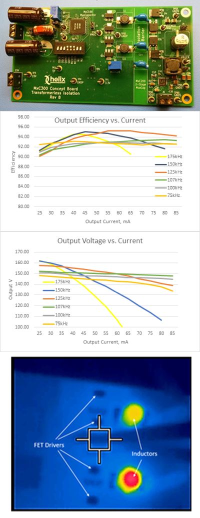
The concept board design shown here is limited by primary and secondary side electronics to 10 W operation at ~125 kHz switching frequency. However, the basic topology used for the capacitive isolation barrier would support a maximum power transfer of 65 W. Adjustments would need to be made to support higher power and voltages. Switching frequencies and the capacitors, inductors, and drivers will need to change.
In realizing this test board, silicon using existing lower-voltage MuxCapacitor stages was used. Because of voltage and power limitations of the silicon available, circuit operation doesn’t entirely represent what a final product would be able to do. The voltage ratings for the MuxCapacitor devices used limit the acceptable voltage across the isolation barrier. The MuxCapacitor blocks use existing silicon made with the X-FAB XDM10 (primary side) and XT018 (secondary side) processes. The maximum voltage allowed for some components on the secondary side is 60 V. The final product will use a 400-V process and 300 V across the barrier. For the isolation barrier testing, the lower-voltage secondary side components were bypassed so voltages up to 200 V could be used.
The prototype board was designed to be a vehicle for UL approval of the touch current and isolation. The maximum input voltage that can be used is limited, so testing consisted of applying 152 V to the input of the modulator and bypassing the voltage conditioning that will be included in final silicon. The output is taken on the secondary side across the dc bulk capacitor after “demodulation” by the full wave bridge. The clock frequency can be varied so the effect of barrier frequency on the operation can be tested. The component values for the isolation coupling consist of two 2.2-nF Y1 capacitors in series with two 1-mH inductors (one capacitor and one inductor in each leg). These have a resonant frequency of 107 kHz.
The circuit performs best when using zero-voltage switching (ZVS). Without the inductors, more power will dissipate in the drivers. The switches have three pertinent parasitics that reduce efficiency: on resistance Rdson, output capacitance Coss, and gate capacitance Cg. The switch timing depends on Rdson and Coss, which determine the required dead time. Without the inductor, the switching losses would be 4CossV+2f, where f is the switching frequency.
This loss can be eliminated using ZVS where the inductor recovers the charge on Coss. The gate has similar losses that are less significant because the gate switching voltage is much lower. With the capacitor and inductor values used, the operation and efficiency can be adjusted by changing the frequency of operation.
For ZVS to work properly, the net impedance of the L/C network must be inductive, so the best operating frequencies are somewhat above the resonance of the coupling network. The observation that the efficiency can be affected by changing the frequency suggests that adjusting the barrier frequency is a way to optimize the overall efficiency.
At 150 kHz the best overall efficiency (95%) is measured at 45 mA. From 50 to 65 mA the highest efficiency (95.25%) is at 125 kHz. Reducing the barrier frequency nearer the resonance point reduced the peak efficiency, and the efficiency across the different loads became flatter. Though the circuit is not operating at resonance, the capacitive and inductive reactance mostly cancel in the L/C network but with some inductive reactance remaining. Operating with only the capacitor would not have this benefit and the losses would be higher.
As the barrier frequency rises above the resonant point, the output voltage drops with rising output current. Operation above 150 kHz did not help the performance and significantly reduced performance at 175 kHz compared to performance at 125 and 150 kHz, especially the output voltage vs. output current. When operating the barrier near the resonant frequency, the output voltage and efficiency are relatively flat over the range of currents tested, but the efficiency is lower than when operating at frequencies somewhat higher than the resonant frequency. This means the barrier frequency can be set to optimize the overall efficiency.
Another benefit of ZVS is that the board operates without significant component power dissipation, i.e., heat. The inductors are the warmest components on the board but are only about 50°C at 13 W. ZVS reduces the losses in the other components but boosts the dissipation of the inductors. Using inductors with a lower ESR and higher Q should improve the efficiency.
In all, clearly it is possible to efficiently pass power and provide isolation using capacitors. Additional work is continuing to build a 65-W high-power board and to optimize the components used. Operation at higher voltages and barrier frequencies are planned to boost performance. Passing UL requirements was the first big hurdle and now circuit optimization is underway to make this technique the future of isolation and power transfer.
References
“High Voltage Capacitive Voltage Conversion,” Presented by Neaz Farooqi, Helix Semiconductors, 13:55 17-2 Randall L. Sandusky, Helix Semiconductors, United States; Alexander Hölke, X-FAB Sarawak Sdn. Bhd., Malaysia, 2018 ISPSD, 30th International Symposium on Power Semiconductor Devices and ICs
Mitchell Kline “Capacitive Power Transfer” Technical Report No. UCB/EECS-2010-155,
www.eecs.berkeley.edu/Pubs/TechRpts/20



Leave a Reply