Automotive electronics depends on power supplies that can handle abuse like load dumps. New ICs are optimized for these extreme environments and can meet stringent vehicle safety standards.
Tony Armstrong, Analog Devices Inc.
THE auto industry expects a transition to autonomous vehicles via both an evolutionary path, where existing cars get there little by little (analogous to Tesla’s autopilot feature), and via a revolutionary path characterized by vehicles that are totally self-driving (like the ones Google is working on). In the next few years, more advanced driver assistance features will be
synchronized to navigation and GPS systems. Companies like Google will gather and accumulate data about every situation a self-driving vehicle might encounter. And mapping companies will intensify the 3D mapping of major cities.
Fully autonomous cars will clearly host numerous electronic systems. The more obvious ones include advanced driver assistance systems (ADAS), automated driving computers, autonomous parking assist, blind spot monitoring, intelligent cruise control, night vision, lidar sensing, and more. All these systems require a variety of different voltage rails and current levels; however, they generally require power directly from the automobile battery or alternator. In some instances, they may be powered from a post-regulated rail derived from one of the main sources. This is usually the case for the core voltages of VLSI digital ICs such as FPGAs and GPUs which can need operating voltages below one volt at currents ranging from a couple of amps to tens of amps.
System designers must ensure that the ADAS systems comply with the noise immunity standards pertaining to vehicles. In the automotive environment, switching regulators replace linear regulators in areas where low heat dissipation and efficiency are valued. The switching regulator is typically the first active component on the input power bus line, so it has a significant impact on the EMI performance of the complete converter circuit.
In the case of conducted emissions, the noise is localized to a specific terminal or connector in the design. Compliance with conducted emissions requirements can often be assured relatively early in the development process with a good layout or filter design. However, it can be more difficult to minimize radiated emissions because every trace on the board is potentially an antenna and every copper plane is a resonator. Even with careful design, power supply designers never really know how bad the radiated emissions will be being until the system gets tested. And radiated emissions testing cannot formally take place until the design is essentially complete.
Filters are often used to reduce EMI by attenuating the strength at a certain frequency or over a range of frequencies. A portion of this energy that travels through space (radiated) is attenuated by adding metallic and magnetic shields. The part that rides on PCB traces (conducted) is tamed by adding ferrite beads and other filters. EMI cannot be eliminated but can be attenuated to a level that is acceptable by other communication and digital components. Moreover, several regulatory bodies enforce standards to ensure compliance.
Modern input filter components in surface mount technology have better performance than through-hole parts. However, this improvement is outpaced by the increase in operating switching frequencies of switching regulators. Higher efficiency, low minimum on- and off-times result in higher harmonic content due to the faster switch transitions. For every doubling in switching frequency, the EMI becomes 6 dB worse while all other parameters, such as switch capacity and transition times, remain constant. The wideband EMI behaves like a first-order high-pass with 20-dB higher emissions if the switching frequency rises by a factor of ten.
Savvy PCB designers will make the hot loops small and use shielding ground layers as close to the active layer as possible. Nevertheless, device pin-outs, package construction, thermal design requirements and package sizes needed for adequate energy storage in decoupling components dictate a minimum hot-loop size. To further complicate matters, in typical planar printed circuit boards, the magnetic or transformer style coupling between traces above 30 MHz will diminish all filter efforts because the higher the harmonic frequencies are, the more effective unwanted magnetic coupling becomes.
EMI cannot be eliminated but can be attenuated to a level that is acceptable. The usual approach is with tuned filters, metallic and magnetic shields, and ferrite beads. These components, of course, add cost.
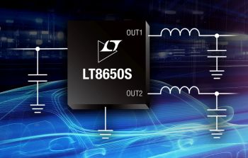
These factors are among the reasons IC makers have devised special components aimed at producing power rails on connected vehicles. An example is the LT8650S – capable of working with high input voltages, it is a dual-output monolithic synchronous buck converter that also has low EMI/EMC emissions. Its 3-to-42-V input voltage range makes it a candidate for automotive applications, including ADAS. One of the requirements for handling ADAS is an ability to regulate through cold-crank and stop-start scenarios with minimum input voltages as low as 3 V and in the presence of load dump transients in excess of 40 V.
This chip’s dual-channel design consists of two high-voltage 4-A channels, delivering voltages as low as 0.8 V, thus giving it the ability to drive the lowest-voltage microprocessor cores currently available. Its synchronous rectification topology delivers up to 94.4% efficiency at a switching frequency of 2 MHz, while Burst Mode operation keeps quiescent current under 6.2 µA (both channels on) in no-load standby conditions making it a good candidate for always-on systems.
As a quick review, Burst Mode technology allows a switch-mode power supply to operate efficiently even when lightly loaded. It does so by turning off non-essential circuitry when the output is in regulation. Meanwhile, a comparator actively monitors the output so the control circuitry can quickly turn on when the output begins to droop. As the load current rises, the converter will automatically transition between Burst Mode to the lower-noise PWM mode of operation. Conversely, the converter will automatically transition from PWM to Burst Mode operation when the load drops.
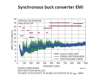
The LT8650S switching frequency can be programmed from 300 kHz to 3 MHz and synchronized throughout this range. Its 40-nsec minimum on-time enables 16 Vin to 2.0 Vout step-down conversions on the high voltage channels with a 2-MHz switching frequency. This chip has what’s called a Silent Switcher 2 architecture designed to minimize EMI. It does so through, among other things, use of two internal input capacitors as well as internal barium strontium titanite (BST) and INTVCC (voltage powering the IC gate driver and control circuit) capacitors to minimize the area of the hot loops. Other features designed to minimize EMI include well-controlled switching edges and an internal construction with an integral ground plane and the use of copper pillars in lieu of bond wires.
Moreover, the EMI/EMC performance is not sensitive to board layout. The LT8650S can easily pass the automotive CISPR25, Class 5 peak EMI limits with a 2 MHz switching frequency over its entire load range. Spread spectrum frequency modulation is also available to lower EMI levels further.

Another example of a chip intended for automotive use is the LT8645S. It targets applications needing a wider input range. It is a monolithic synchronous buck converter that also has low EMI emissions. Its 3.4 to 65-V input voltage range makes it a good candidate for both automotive and truck applications which must regulate through cold-crank and stop-start scenarios with minimum input voltages as low as 3.4 V and load dump transients exceeding 60 V. It is a single-channel design, delivering an 8-A output at 5 V. Its synchronous rectification topology delivers up to 94% efficiency at a switching frequency of 2 MHz, while Burst Mode operation keeps quiescent current under 2.5 µA in no-load standby conditions, making it work well for always-on systems.
The LT8645S switching frequency can be programmed from 200 kHz to 2.2 MHz and synchronized throughout this range. Like the LT8650S, it
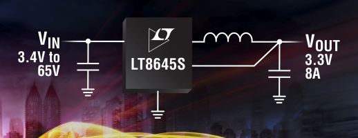
incorporates features that minimize EMI and can easily pass the automotive CISPR25, Class 5 peak EMI limits over its entire load range. Spread-spectrum frequency modulation is also available to further lower EMI levels.
The LT8645S utilizes internal top and bottom high-efficiency power switches with the necessary boost diode, oscillator, control and logic circuitry integrated into a single die. Low ripple Burst Mode operation maintains high efficiency at low output currents while keeping output ripple below 10 mV p-p. Finally, the LT8645S sits in a small thermally enhanced 4×6-mm 32-Pin LQFN package.
In the future, voltage and current levels needed for automotive circuits are likely to change; nevertheless, the requirements for low EMI/EMC emissions will not go away nor will the hostile environment in which they must operate. But, in the not too distant future, we will be able to sit back, relax and enjoy our car taking us for a ride.





Leave a Reply