The power density of point of load (buck) converters (PoLs) has been increasing for several decades. It is driven by a combination of component improvements and advanced power conversion technologies that produce the increases in power conversion efficiencies needed to support higher power densities. Where are we now? And what’s next?
Power density is an important parameter to consider when comparing various power converter designs. It can be measured in many ways: Watts per cubic inch or cubic millimeter; Watts per pound or kilogram; cubic inches or cubic millimeters per Ampere; and so on. However it’s measured, the power density of PoLs has been on increasing over an extended period of time.

Buck basics
A buck converter topology used in PoLs includes a controller, two semiconductor devices, and at least one energy storage element, either a capacitor or an inductor, or, more commonly, both a capacitor and an inductor as the output filter. A basic buck converter uses one power MOSFET and a rectifier, which could be a Schottky diode. A newer and more efficient approach, called a synchronous buck, replaces the output rectifier with a synchronous rectification MOSFET. In a typical PoL buck converter, the percentage of time that the power MOSFET is on during a switching cycle is called the duty cycle and is equal to the output voltage ratio to the input voltage.

Efficiency improvements are a key element enabling increasing PoL power densities. Common sources of losses in PoL buck converters include:
- Switching losses in the power MOSFET(s)
- Conduction losses in the power semiconductors (diode forward drop and MOSFET RDSon)
- Inductor winding resistance and ac losses
- Capacitor equivalent series resistance
Component improvements that reduce these sources of inefficiency are the drivers of increased power densities on PoLs. Improved packaging and thermal management are second-order factors driving higher power densities.
Power switch trends
On resistance (RDS(on) and gate charge (Qg) are two key performance metrics for power MOSFETs. The power MOSFET figure of merit (FOM), RDS(on) x Qg, is still widely used to compare various devices. However, today’s power MOSFETs are highly developed devices and have an optimized Qg that works with today’s advanced gate drivers. The tradeoff between larger device size with lower RDS(on) and smaller device size for lower Qg still applies, and power MOSFETs continue to have better FOMs. But that progress is much more incremental, and there is another parameter that has also become the focus of further improvements in power MOSFET performance, Qrr.
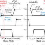
Qrr is the reverse recovery charge in the PN junction of the MOSFET body diode when the diode is forward biased. Qrr results in dissipation which lowers efficiency. In addition, Qrr can impact voltage spiking, resulting in increased electromagnetic interference and even device failure. The importance of Qrr increases at higher switching frequencies.

As improvement in power MOSFET performance becomes increasingly difficult to achieve, efforts to develop better packages with lower parasitics have taken on more importance. For example, suppliers are offering co-packaged high-side and low-side MOSFETs for use in PoLs. Elimination of one package contributed to higher converter power densities, simplified PCB layouts, and better PoL performance.
Inductor trends
After the power MOSFETs, the inductor is the next-most dissipative component in a synchronous buck converter, and the inductor DC resistance (DCR) is an important consideration. Unlike the power MOSFETs, which turn on and off, the inductor is always conducting current.
Recent inductor developments include high-performance devices with up to 40% lower DCR and low AC losses that result in significant efficiency improvements. These devices have been optimized for PoLs with switching frequencies ranging from hundreds of kHz to 5 MHz.
GaN enables high-density PoLs
While silicon MOSFETs continue to improve incrementally, gallium nitride (GaN) power switches can enable a step-function improvement in PoL power densities. For example, a GaN-based asymmetrical half-bridge has been developed that is rated at 30V and 16A with an on-resistance of 19 mΩ for the upper FET Q1 and 8 mΩ for the lower FET Q2. The GaN switches have much lower parasitic capacitances than silicon FETs, resulting in low switching losses, even at frequencies as high as 10MHz. With a footprint of about one-seventh the area of comparable silicon MOSFETs, this GaN IC can be used to design a 1V/12A synchronous buck converter PoL with a power density of 1000 W/in3. The high switching frequency of this PoL reduces filtering needs and allows the use of a much smaller output inductor with lower losses.

Enabling an even higher level of integration, GaN-based integrated voltage regulators (IVRs) eliminate or integrate all discrete components into a single device. A 10A IVR can maintain regulation through a load step from zero to 10A in 500ns with <15mV droop without the need for external output capacitors. These IVRs have peak efficiencies of up to 92% with a nearly flat efficiency curve. A three output IVR has been integrated into a 5mm x 5mm package with a 0.75mm profile that delivers up to 10x higher power density, 3x tighter accuracy during transients than previous solutions.
GaN IVRs can enable power savings of 10% or more with similar reductions in heat dissipation. In addition, these dc/dc converters support 1,000x faster dynamic voltage scaling compared with conventional power management IC (PMIC) based PoLs, enabling fast and lossless processor state changes that can save 30% or more of the processor power.

Hybrid architecture supports smaller PoLs
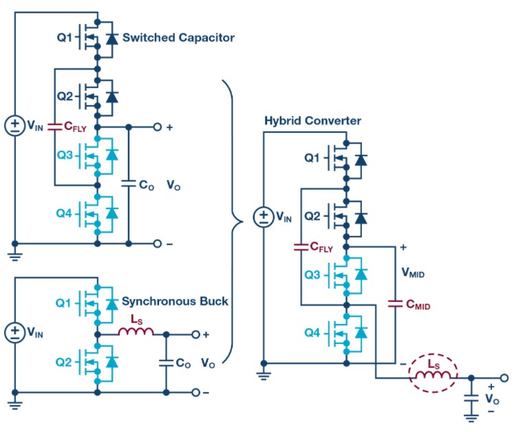
A common distributed power architecture uses isolated intermediate bus converters to convert the 48Vdc power distribution bus to a lower 12Vdc intermediate bus, using what is referred to as intermediate bus converters (IBCs) that feed the PoLs. In applications such as 48V automotive systems and power distribution in data centers and telecommunications central offices, the 48Vdc bus is already isolated, eliminating the need for isolated IBCs. When there is no need to isolate the intermediate bus, the conventional IBCs can be replaced using a hybrid solution consisting of a switched capacitor (SC) converter and a synchronous buck converter. The SC converter steps down the input voltage by 50%, reducing the input-to-output voltage ratio of the buck converter and improving efficiency.
A hybrid SC-buck can operate at 3x higher switching frequency while delivering the same overall efficiency as a conventional buck, enabling a reduction of the overall solution size up to 50%. The hybrid SC-buck can deliver up to 3% efficiency improvement if operated at the same frequency as a conventional buck PoL. The hybrid SC-buck approach’s additional benefits include eliminating the inrush current usually associated with SC converters prebalancing the capacitors on startup and low EMI emissions due to a soft-switched front end.
Summary
The power densities of PoLs have been increasing for many years, primarily driven by improvements in power MOSFETs and inductors. However, those components are now highly optimized, and continued increases in silicon MOSFET-based PoL power densities are becoming more incremental. That may be changing as a result of new developments in GaN power switches and GaN power ICs. At the same time, creative power conversion solutions such as hybrid SC-buck conversion could breathe new life into silicon MOSFET-based PoL solutions.
References
72 V Hybrid DC-to-DC Converter Reduces Intermediate Bus Converter Size by up to 50%, Analog Devices
Inductor Selection Guide for Buck Converters, Magno Teknik
Integrated inductors empower multiphase buck converters for computing, Eaton
New High-Performance Power Inductors Reduce DC Resistance by up to 40%, Coilcraft
Qrr: overlooked and underappreciated in efficiency battle, Nexperia
Understanding the Trade-offs and Technologies to Increase Power Density, Texas Instruments
What is an Integrated Voltage Regulator (IVR)?, Empower Semiconductor


Leave a Reply