by Akshay Mehta and Yang Zhang, systems and applications engineers, Texas Instruments
DC/DC converters are often used in distributed power-supply architectures for industrial applications. Many architectures use two types of output capacitors: One has higher capacitance and higher equivalent series resistance (ESR), such as aluminum electrolytic, while the other has much lower ESR and relatively lower capacitance, such as ceramic capacitors. Architectures using mixed-type capacitors at the output can be grouped into two sections:
- In a typical distributed-power-supply architecture for FPGA-based applications, a wide VIN regulator converts a high-voltage rail to downstream low-voltage rails. Now the upstream rail output capacitors become the downstream rail input capacitors. Therefore, the downstream rail ceramic input capacitors and the upstream rail electrolytic output capacitors create a mixed-type capacitor situation for the upstream rail.
- Bulk capacitors with high ESR provide the required amount of output capacitance given their lower cost, size and availability. Additional ceramic capacitors can improve the steady-state output-ripple voltage and transient performance.
In this article, we address the effect of mixed-type output capacitors on voltage ripple and loop response and how your selection of mixed-type capacitors affects DC/DC regulator performance. We analyze the combined impedance of ceramic and electrolytic capacitors and list the basic steps involved in calculating the open-loop transfer function for a voltage-mode buck converter.
Impedance of mixed-type capacitors
Depending on the design requirement, the output of a voltage regulator may require bulk capacitance. While new technology does exist to give devices more capacitance along with much lower parasitic ESR, the availability and cost-effectiveness of aluminum electrolytic (Al-El) capacitors are still unbeatable. This combination makes Al-El capacitors ubiquitous in DC/DC voltage-regulator applications. The main drawback of these capacitors is that the ESR is typically very high at much lower frequencies, and often these capacitors are not well-documented in the datasheets.
Let us look at the frequency response of a single 100-µF Al-El capacitor that has about 100 mΩ of ESR.
The zero caused by the capacitance, C1, and its ESR, R1 (Figure 1) is given as Equation 1.
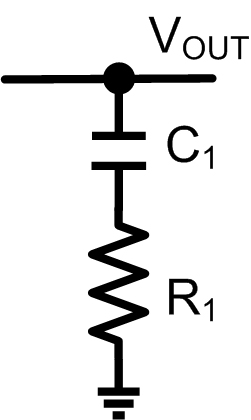
Knowing that C1 is 100 µF and R1 is 100 mΩ, you can calculate the ESR zero frequency, fZERO, to be around 15 kHz. If compensation of the DC/DC regulator is done without considering the effect of the electrolytic capacitor’s ESR, then this additional zero can throw the stability out of balance.
To mitigate the effect of a high-ESR bulk capacitor, additional ceramic capacitors can help – but only to a limited extent. Consider adding just one ceramic capacitor as shown in Figure 2.
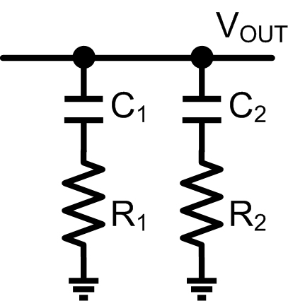
The impedance measured on the bench shows that the ceramic capacitor, C2, is 2.2 µF and has a very low ESR, R2, of 5 mΩ. The zero frequency of C2 fZERO2 calculated by Equation 1 is about 14 MHz. When these two are paralled at the output of a converter, does the ceramic capacitor nullify the low frequency zero caused by the electrolytic capacitor’s ESR? This can only be verified by some further analysis.
Let us now look at the combination of the two capacitors. Equation 2 shows the impedance of the parallel capacitor network:
Equation 2 shows that in addition to the two zeros from the two capacitors, there is an additional pole caused by the total ESR, RT, and the series combination of the two capacitors, CS (Equation 3):
Therefore, when placing one 2.2-µF ceramic capacitor in parallel with a 100-µF electrolytic capacitor, Equation 6 calculates the additional pole at about 700 kHz. This high-frequency pole cannot compensate the low-frequency fZERO1 and cannot help in the event of instability. Therefore, adding just a single 2.2 µF ceramic capacitor does not nullify the effect of the electrolytic capacitor’s ESR.
In order to actually mitigate the effect of high ESR from the electrolytic capacitor, you would have to add additional low-ESR ceramic capacitors. Adding three more capacitors gives you a total of about 10 µF with low ESR. The capacitor pole as described in Equation 3 now moves in at lower frequencies, and the phase gain from the higher-ESR zero is compensated at relatively lower frequencies. So, yes, the ceramic capacitor does nullify the low frequency zero caused by the electrolytic capacitor’s ESR.
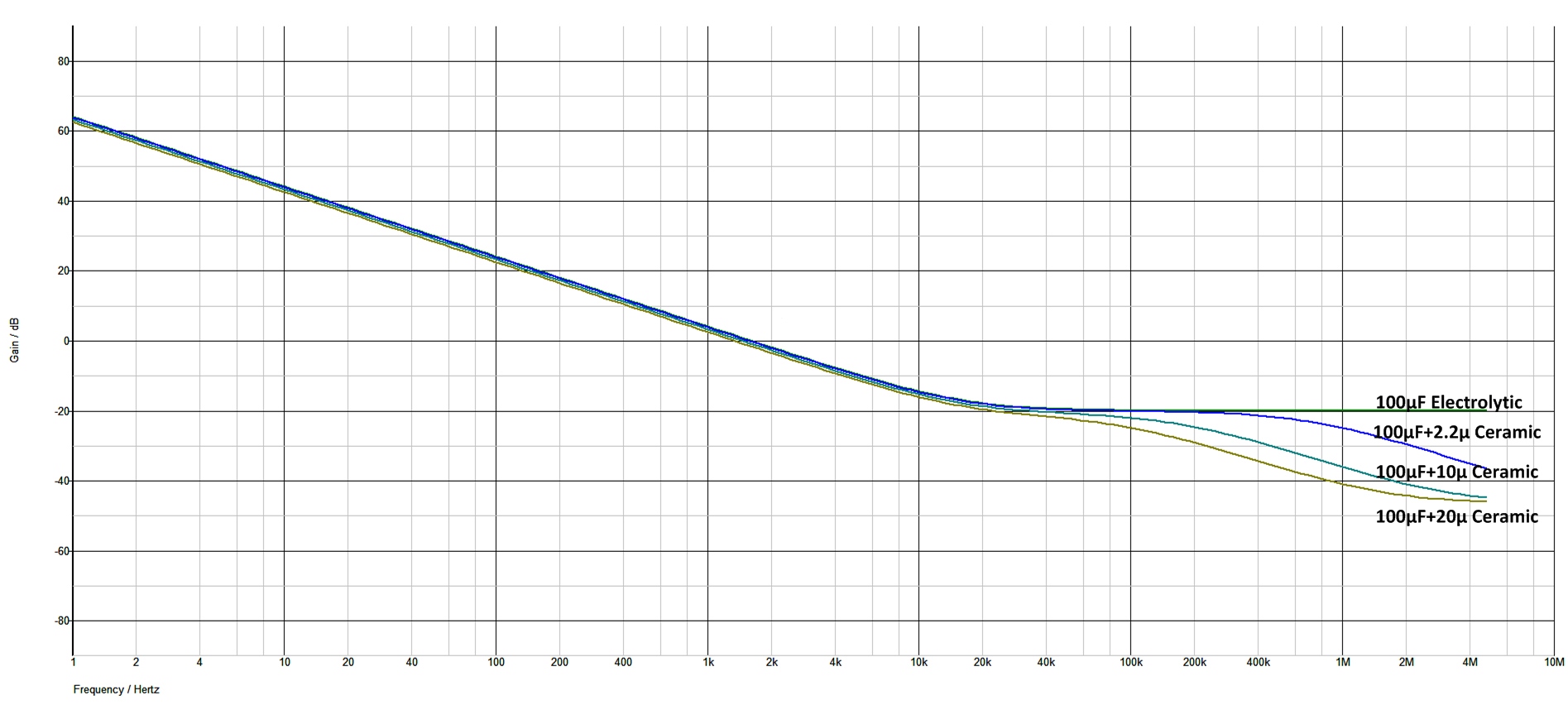
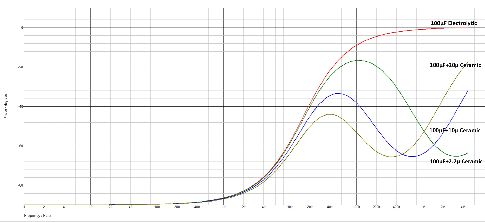
Figure 3 and Figure 4 show frequency-response plots for combinations of electrolytic and ceramic capacitors. These figures show that adding more ceramic capacitors can help to reduce the frequency of the additional pole and compensate for the low-frequency ESR zero. The plots show additional 2.2-µF, 10-µF and 20-µF ceramic capacitors in addition to the 100-µF electrolytic capacitor. These figures also show that the ESR of the combined capacitors is reduced at lower frequencies. This can help reduce the steady-state voltage ripple at high switching frequencies, as we will explain in the next section.
Vout ripple analysis
Equation 4 expresses the impedance of each capacitor as:
Where the real part, R, equals the ESR resistance, and the imaginary part is the reactance (Equation 5):
You can also express the impedance with Equation 6:
Where the magnitude is and the phase is|Z|=√(R2+X2 ) and the phase is θ(Z) = atan (X/R)
Equations 7 and 8 calculate the magnitude and phase, respectively, of the two paralleled capacitors shown in Figure 2:
You can then back-calculate the effective capacitance and ESR of the paralleled capacitors based on the magnitude and phase at a particular frequency of interest, f, using Equations 9 and 10:
Referring back to the example case – a 100-µF Al-El capacitor with 100 mΩ of ESR and a single 2.2-µF ceramic capacitor with 5 mΩ of ESR – the effective capacitance and ESR at an assumed 1-MHz switching frequency, f, can be calculated as 4.82 µF and 25 mΩ.
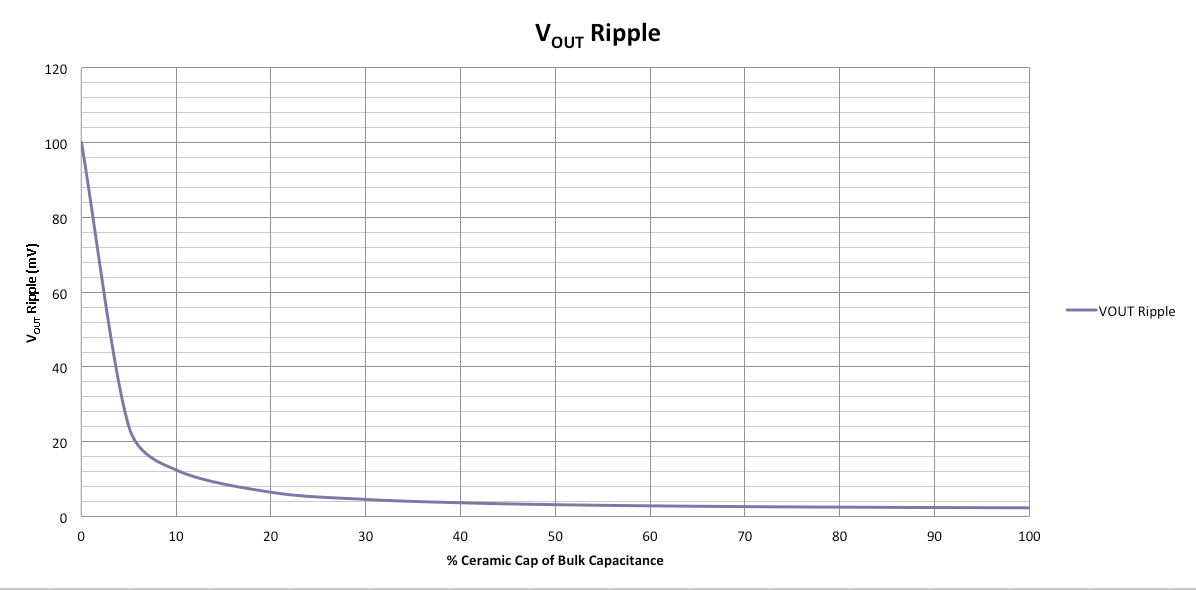
Assuming that the ILPP (peak-to-peak inductor current) is about 1.2 A for a 2.5-V regulated DC output, Equation 11 calculates the root-mean-square (RMS) output-voltage ripple at the output of the DC/DC regulator to be about 44 mV. The same example with four 2.2-µF ceramic capacitors gives you about 12 µF with only 3-mΩ effective ESR. The resulting VORIPPLE is now only 13 mΩ.
Figure 5 illustrates this graphically. The plot shows the effect of more ceramic capacitors on the steady-state output-voltage ripple.
Figure 5: Output voltage ripple versus increasing ceramic capacitance.
The switching frequency for the example described is set to 1 MHz The requirement of extra ceramic capacitors changes based on the converter’s switching frequency. At lower switching frequencies, the equivalent ESR would be higher, as would the resulting ripple at the output. Therefore, if the converter’s chosen switching frequency is lower, bringing the output ripple down requires adding ceramic capacitors at the output.
The chart in Figure 6 shows the ripple voltage versus frequency for three cases. It exemplifies what happens to the output-voltage ripple over frequency with ceramic capacitors of different values.
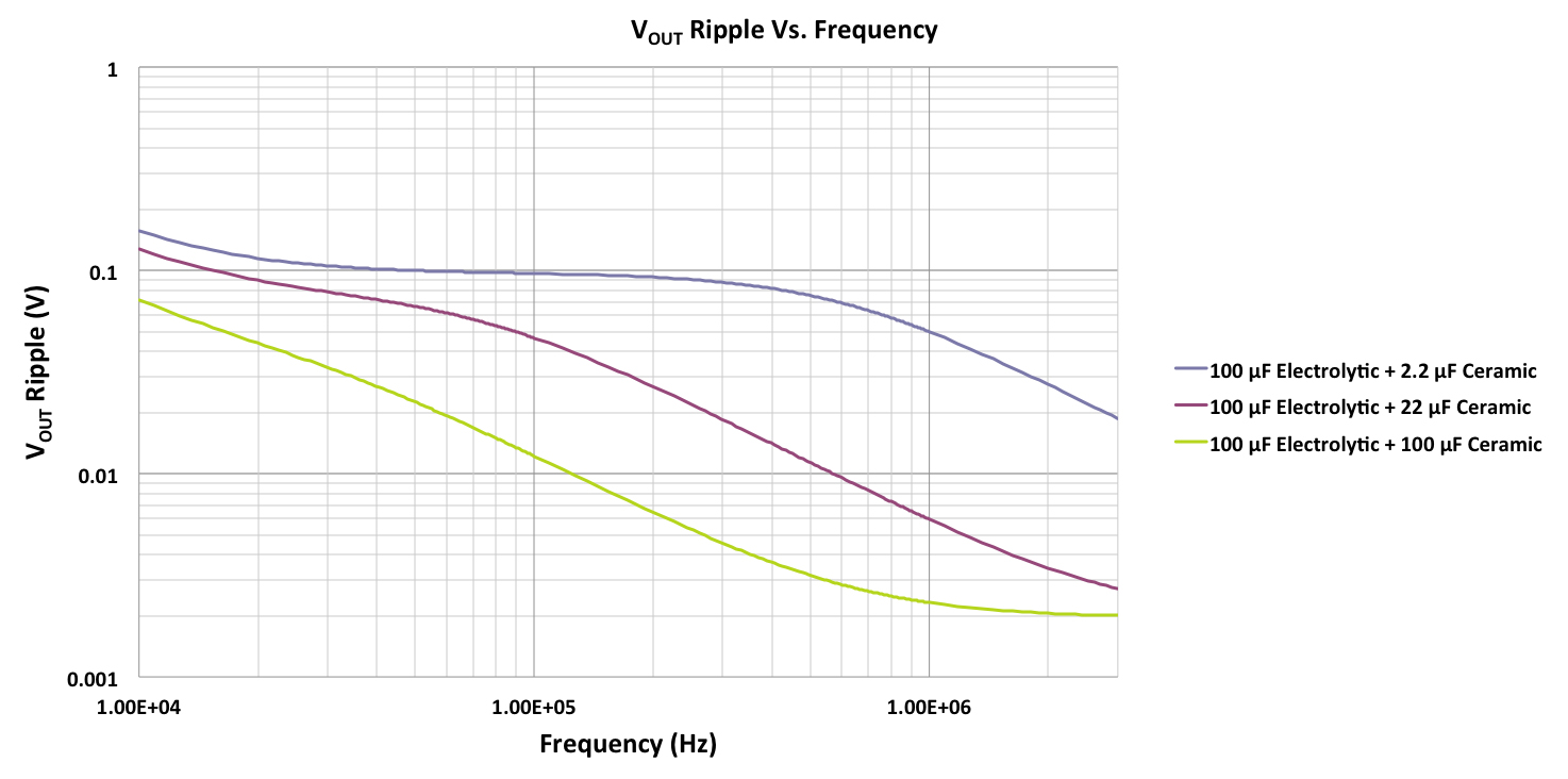
Figure 6 also illustrates that at lower frequencies, it helps to have more ceramic capacitors in parallel with a bulk electrolytic capacitor.
Effect of mixed-type output capacitors on loop compensation
Various technical papers and device data sheets have documented the calculation of compensation components for DC/DC converters; therefore, we will not repeat this information. Our goal is to understand how the open-loop transfer function changes when there is an additional mixed-type capacitor at the output of a DC/DC regulator. Understanding the open-loop transfer function is the first step in calculating the compensation components. We use a voltage-mode buck topology for our example.
Single output capacitor. We start by looking at the uncompensated L-C tank-loop response as shown in Figure 7.
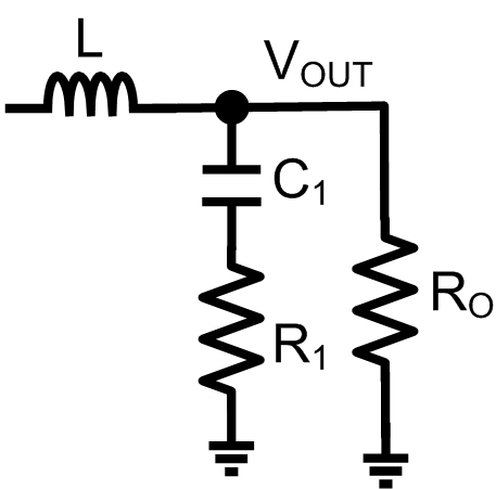
This response depends on the input voltage, internal ramp amplitude, L and C values, and their parasitics. For a single capacitor at the output, Equation 12 shows the open-loop transfer function, TOL:
Where
VIN = input voltage to the buck converter
VRAMP = amplitude of the internal sawtooth ramp presented to the pulse-width modulation (PWM) comparator
The effective Q and frequency of the double pole depend on RO, L, C1 and R1, as shown in Equations 13 and 14. Equation 15 shows the zero frequency caused by the capacitor and its ESR:
Two parallel output capacitors. Next we look at the uncompensated L-C tank-loop response for the mixed-type output capacitors as shown in Figure 8.
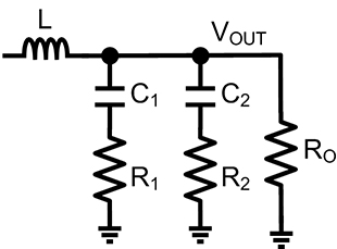
In the case of two parallel capacitors, adding subsequent capacitors can cause instabilities, if you do not consider the total output capacitor impedance.
To correct for this, we have to revisit the equations that apply to a single-output capacitor. For the same voltage-mode regulator, if you now have one bulk electrolytic capacitor and one lower-value ceramic capacitor, the open-loop transfer function changes (Equation 16):
where Rt = R1+R2 and Ct = C1+C2.
As you can see from Equation 16, the complexity of calculations increases rapidly when adding mixed-type capacitors.
Solving the equation analytically can be quite tedious. You can use your preferred SPICE tool to plot the transfer function over frequency. The subsequent steps to calculate compensation components would remain the same.
Let us look at an example to better understand this situation. The LMZ10504 is a highly integrated DC/DC module. The design inputs are: VIN = 5 V; VOUT = 1.2 V
and IOUT = 4 A.
The design has two output capacitors. COUT1 is a 100-µF electrolytic capacitor with 100 mΩ of ESR. COUT2 is a 22-µF ceramic capacitor with 3 mΩ of ESR. You can plot the power-stage gain using an averaged model for the LMZ10504. The plot can also help you calculate the compensation components. Figure 9 shows the power-stage gain and phase for the design.
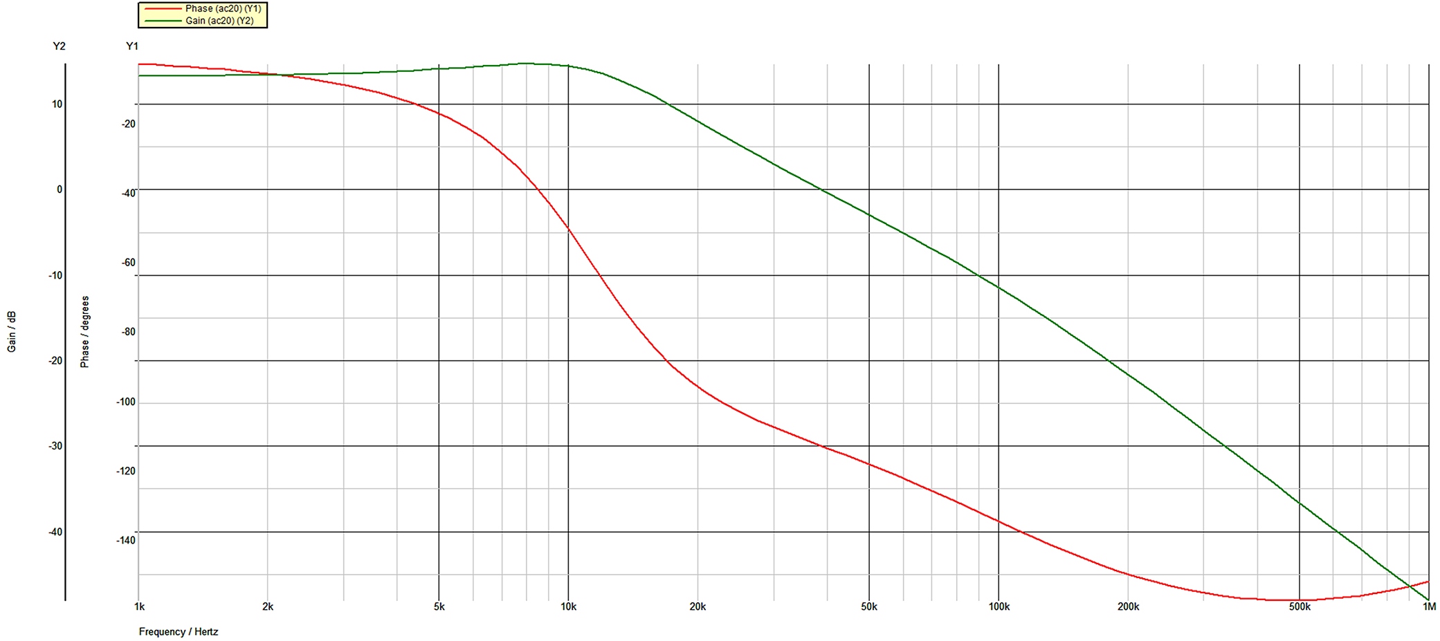
To calculate the compensation components, typically you must know the desired crossover frequency and power-stage gain at the desired crossover frequency. The switching frequency of the DC/DC module in our example is 1 MHz. The desired crossover frequency is usually set to a tenth of the switching frequency, or 100 kHz in our example. From Figure 9, you can see that the gain at 100 kHz is roughly about –11 dB. We know that at the crossover frequency the system gain is 0 dB. This means that we need to add 11 dB to the power-stage gain from the compensator to obtain the desired crossover frequency. The relationship is in equation 17
The gain parameter in equation 17 is what we talked about earlier. In our example it is 11 dB. The LMZ10504 has partial internal compensation and the RCINT is the internal compensation resistor of 100 kΩ. Once the upper feedback resistor is calculated from equation 17, the external compensation components can be calculated. [1]
In a different situation, if the compensation components are external to the device, then the upper feedback resistor is preset to obtain the required VOUT along with lower feedback resistor. The compensation resistor, RCOMP, can then be calculated using equation 17.
In this article, we have shown how the use of mixed-type capacitors in DC/DC systems is quite useful. Mixed-type of capacitors at the output can help in reducing ripple. Choosing the right amount of bulk and ceramic capacitance and performing loop analysis on the resulting design is important to maintain system stability.
Akshay Mehta is a systems and applications engineer with Texas Instruments’ SIMPLE SWITCHER® product group, where he is responsible for product definition and development, bench validation, and customer support. Akshay received a master’s degree in electrical engineering from the University of Texas at Arlington. For questions about this article, you can reach Akshay at ti_akshaymehta@list.ti.com.
Yang Zhang is also a systems and applications engineer with the SIMPLE SWITCHER® product group at Texas Instruments, where she also is responsible for product definition and development, bench validation, and customer support. Yang received a Ph.D. from the University of Colorado at Boulder and electrical engineering undergraduate degree from the Tsinghua University, Beijing, China.
References
- Yang Zhang, Akshay Mehta. LMZ1050x/LMZ1050xEXT SIMPLE SWITCHER® Power Module – Quick Compensation Design, Texas Instruments Application Note, September 2015.
- Michael Score. Ceramic or electrolytic output capacitors in DC/DC converters – Why not both? Texas Instruments Analog Applications Journal, 3Q 2015.
- Download the LMZ10504 data sheet.




Why in Fig 4 does gain slope down to -20 dB and go level? A zero slopes positive and a series RC has high negative gain (attenuation) at low frequencies and levels out to the constant value of ESR at high frequencies. Gain doesn’t seem to apply to me for a shunt impedance across an output voltage.