(Editor’s note: check out the full article, “The fundamental advantages of D-Mode GaN in cascode configuration,” and get the full technical story behind these “busted” myths.)
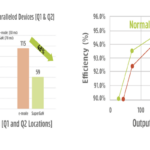
Reality: In cascode GaN technology, the GaN chip bears most of the off-state high voltage (> 90%). The Si MOSFET needs only to bear a few 10s of volts. And, as the specific on-state resistance per unit area decreases quadratically with rated voltage, the Si MOSFET achieves incredibly low RDS(on), less than 10% of the total cascode resistance, and a very small reverse recovery charge (Qrr). Notably, Qrr is an order of magnitude lower than high voltage superjunction Si MOSFET technology. To put things in perspective, if we take a conventional 600 V Si superjunction power device, the resistance-versus-charge figure of merit (Ron * Qrr) is 145 mΩ-pC. If we take a 650 V GaN cascode, the figure of merit drops to 6 mΩ-pC, marking a huge improvement. And of 6 mΩ-pC, the low voltage Si MOSFET contributes only 0.5 mΩ-pC — less than 10% of the total cascode, and less than 0.5% of the 600 V silicon power device (Figure A). Myth busted!
More myths
Myth #2: e-mode devices have no Qrr
Yes, GaN HEMTs have no reverse conduction bipolar transport, but completely eliminating Qrr? Think again.
Myth #3: Cascode GaN oscillates
Read how following standard design principles enhances performance and suppresses oscillations and EMI.


Leave a Reply