A few simple thermal management guidelines can help conduct heat away from GaN FETs.
Assaad Helou, Efficient Power Conversion
Enhancement-mode gallium nitride (eGaN) FETs offer high power-density with ultra-fast switching and low on-resistance, all in a compact form factor. However, the power levels these high-performance devices provide can be limited by extreme heat-flux densities. If not managed properly, the generated heat can compromise reliability and performance. Fortunately, chip-scale packaging for eGaN FETs can be leveraged at the board-side and the backside (i.e., case) to better dissipate heat.

Packaged electronic devices dissipate the heat they generate through two main paths – to the printed circuit board (PCB) at the board-side and to the case at the backside. Both avenues can benefit from thermal management strategies.
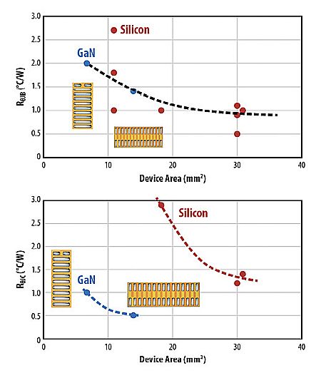
Heat generated within the FET encounters its first thermal resistances from the semiconductor junction to the PCB (RθJB) and from the junction to the transistor case (RθJC). These two thermal resistances, usually given in °C/W or °K/W, differ for each FET because they depend on the device construction and the thermal conductivity of the materials used. For wafer level chip-scale packaged (WLCSP) GaN FETs, the RθJC is lower than for silicon devices. But both RθJC and RθJB can be used to significant advantage.

Semiconductor device makers typically report the maximum temperature rise (in °C or °K), and the resulting overall thermal resistance for the maximum temperature at the device junction with reference to an ambient temperature in still air (RθJA) or in moving air (RθJMA). The thermal resistance to the board is one component in a network of heat conduction paths that determines the overall self-heating in a GaN FET device.
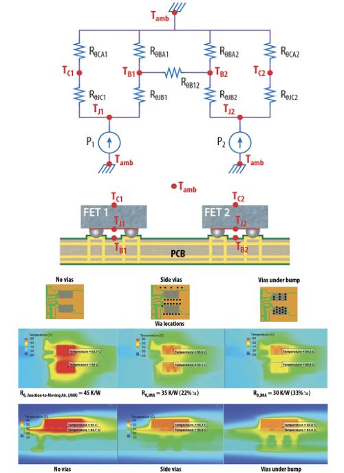
A simplified circuit model representing the main heat conduction paths from the junction to ambient on a standard PCB contains four thermal resistances: In addition to RθJC and RθJB mentioned previously, there are thermal resistances from the case to the ambient, RθCA, and from the PCB to ambient, RθBA. Additionally, when two heat-generating devices sit near each other on the PCB, there may be another thermal resistance between their mounting points on the PCB, RθB12. Because the FET area is much smaller than that of the PCB, the heat dissipated from the FET to ambient through the case is minimal, so thermal resistance RθCA is large. As a result, without any back-side cooling, the main heat dissipation path from the FET is through the PCB. This explains why good thermal conductance at the board-side must be ensured.
Heat conducts from the FET into the board mainly by the copper traces within the conducting layers of the PCB. Thus it is helpful to specify PCB traces that are thicker not only for low electrical resistance but also for better heat conduction at each layer of the PCB. For example, two-ounce copper layers have twice the conductance of one-ounce layers in the lateral directions. Moreover, the in-plane heat conductance depends proportionally on the number of PCB layers because more layers offer more paths to dissipate heat.
In the through-plane direction, the insulating dielectric layers separating the copper layers have a low thermal conductivity and thus obstruct heat dissipation. Heat conduction can be partially improved by placing vias beneath or near the FETs. The vias provide a path with high thermal conductivity that bridges the dielectric layers and carries generated heat into the inner copper layers of the PCB. The inner layers, in turn, help spread heat, further reducing RθJB and RθJA. Strategically placed thermal vias near or under the FET pads can reduce self-heating (ΔT) by up to 33%.
Improving junction-to-case dissipation
Heat also dissipates from a wafer level chip-scale packaged (WLCSP) GaN FET device die through the case which offers a much lower resistance (RθJC) than the board-side and lower than other types of packaged devices. The exposed die area of the FET is too small for any significant thermal exchange with the surrounding air, so implementing simple thermal management strategies can improve backside cooling considerably.

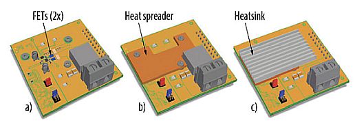
The addition of a heat spreader in contact with the die provides a path for conducting heat in the lateral direction. The heat spreader increases effective surface area of the device and reduces its operating temperature. A heat sink can be added to the heat spreader to further enlarge the area of heat exchange area with ambient air. The heat spreader and heatsink typically use high conductivity materials, such as aluminum and copper, to ensure optimal performance.

A simple and assembly-friendly approach to attaching a heatsink to GaN FETs and ICs uses a thermal interface material (TIM) to enhance the thermal conductivity at the interface between the device and the heatsink, as well as to provide electrical insulation. An SMD spacer between the heat sink and the PCB maintains the right spacing between the heatsink and the GaN device for the TIM and provides sturdy mechanical attachment for the heatsink. Obviously, components taller than the SMD spacers must be excluded from under the heatsink.
Heat spreader/heatsink attachments added for backside cooling introduce several interfaces that impede heat conduction due to surface roughness and thermal contact imperfections. Moreover, air gaps between the components and attachments don’t conduct heat well. TIMs improve thermal contact and provide good conductance at the interface. TIM can come in several forms, including pads, gels, and liquid gap fillers.
The choice of a TIM involves several selection criteria. Perhaps most obvious, the TIM must have good thermal conductivity (κ) and low thermal resistance to conduct heat . A rule of thumb for κ is > 3 W/m·K. TIMs with higher performance reaching κ > 15 W/m·K are available but more expensive and can be used at the FET interface.
The electrical resistivity is also important for the GaN FET die because the upper FET case will be at switch (SW) node potential and must be electrically isolated from the thermal components. T-Global A1780 and A6200 TIMs are examples for thermally and electrically compliant TIMs with high and moderate κ = 17.8 W/m·K and 6.2 W/m·K respectively.
Another consideration for selecting TIM is the compression force exerted on the die for a certain compression rate (thickness percentage given in the materials’ datasheets). The compression force must not exceed the stress limit of the GaN FETs. Generally, larger devices can withstand higher force. Land grid array (LGA) devices can withstand higher force than equivalent ball grid array (BGA) devices of the same size. The maximum recommended pressure on eGaN FETs and ICs is 40 psi/mm2 of the total bump area and 50 psi for GaN devices in general, based on testing results.
Given the small scale of eGaN FETs, the area of their die sides is comparable to that of the top and bottom surfaces. Thus the sides can contribute considerably to heat conductance. For instance, the 0.9×0.9×0.625-mm EPC2038 FET die has a top and bottom surface area of 1.62 mm2 with the four sides measuring 2.25 mm2 in total. As a result, the four sides can also be used to help dissipate heat, usually by adding a gap filler material around the sides of the FET, such as the GF4000 liquid gap filler from Bergquist (κ = 4 W/m·K).

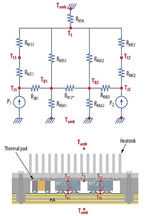
Now consider a resistive circuit model modified to include additional thermal resistances representing the heat conduction from the case to the sink (RθCS) and from the sink to ambient (RθSA). The board also connects to the sink through the metal shim, spacers and gap filler. Also, heat conducts between the board and sink and is represented by RθBS. Though this model contains more thermal resistances than the previous example, the combined thermal resistances of RθCS and RθSA are ideally much lower than RθCA. Thus, the overall effect is less total thermal resistance.
An example of how attaching a heat spreader and heatsink improves thermal dissipation can be seen in the EPC9097 development board. It contains two EPC2204 GaN FETs which are considered major heat sources that must be cooled. There are multiple scenarios for cooling these devices. First, consider the case where a copper heat spreader (κ ≈ 400 W/m·K) is attached to the board using M2 screws and SMD spacers. The high-performance TG-A1780 TIM (κ = 17.8 W/m·K) sits between the FETs and the heat spreaders. Now consider an alternative approach where an aluminum heatsink is attached to the heat spreader using the same type of TIM. Power losses of 1 W are assigned to each FET. The PCBs are placed in 400 LFM air flow at 20°C for forced convection cooling.
The two above scenarios can be compared with baseline models where only board-side cooling is present and when vias are placed in various locations. The maximum temperature is extracted from the thermal model and the overall thermal resistance is calculated in reference to ambient temperature for each FET power (1 W). The percentage of heat dissipated from the board-side and from the case-side are also reported to compare the thermal resistance of each path.
 The results of the thermal analysis summarized in the nearby table show that even without backside cooling, improvements to the board design can reduce temperature by 30%. Compared to board-side cooling, adding a heat spreader to the FETs reduces the overall thermal resistance from 34 °K/W to 22 °K/W (about 40%), while a heatsink reduced the overall thermal resistance to ambient to around 15 °K/W (a 60% decrease from baseline). By reducing the thermal resistance to back-side cooling, the

percentage of heat dissipated through the case rose from 2% (baseline) to 45% with a heat spreader and 61% with an attached heatsink. Given that junction-to-sink thermal resistance is at 4.9 °K/W, improving the heatsink (larger fins, more air flow) can reduce the overall thermal resistance even further.
All in all, when limited to board-side cooling, strategically placement of thermal vias under or near the FETs can improve board conductance significantly. This strategy allows heat to dissipate into the board’s inner copper layers more effectively and reduces peak operating temperatures by around 30%. Moreover, with a low junction-to-case thermal resistance of WLCSP eGaN FETs, the backside offers considerable thermal cooling potential.
Simple thermal management strategies, such as attaching a heat spreader or a heatsink, can increase a device’s effective thermal dissipation area. Use of these measures can reduce FET temperatures by up to 60%, as determined by detailed simulations. With good thermal considerations and simple thermal management strategies, small chip-scale devices can be adequately cooled for reliable performance in high-power applications.


Leave a Reply