
The trends in advanced power electronics packaging mirror the overall packaging trends in the electronics industry. Those trends include adopting chip-scale packaging (CSP), 3D packaging, 3D printing (also called additive manufacturing), and advanced thermal management materials. These trends are being heavily influenced by the adoption of gallium-nitride (GaN) and silicon-carbide (SiC) wide bandgap power semiconductors in power electronics.
The references at the end of this FAQ include links to three important conferences on various aspects of advanced power electronics packaging: International Power Supply-on-Chip (PwrSoC) Workshop, 3D Power Electronics Integration and Manufacturing (3D-PEIM) Symposium, and International Workshop on Integrated Power Packaging (IWIPP)
CSP and heterogeneous integration
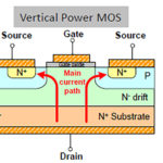
Conventional power semiconductor packages were developed for silicon devices. Since GaN transistors are much smaller than the corresponding Si devices, the packages available when GaN was introduced into the marketplace were much larger than necessary. In addition, they introduced unwanted parasitics that limited the performance of the fast-switching GaN transistors and added undesirable thermal impedance and resistance. In addition, existing packages were developed to accommodate vertical Si power MOSFETs. Lateral GaN enabled and benefited from the development of CSP.
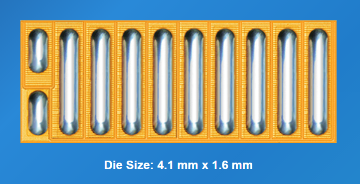
All electrical connections are on the same side of a lateral GaN transistor. For a CSP GaN device, “solderable bars” are placed on the surface of the device. Flipping the part over allows it to be directly soldered to the printed circuit board (PCB). Instead of a plastic molded package, “solderable bars” can be placed directly on the surface of the device. Flip the part over, and it can be mounted directly onto a PCB.
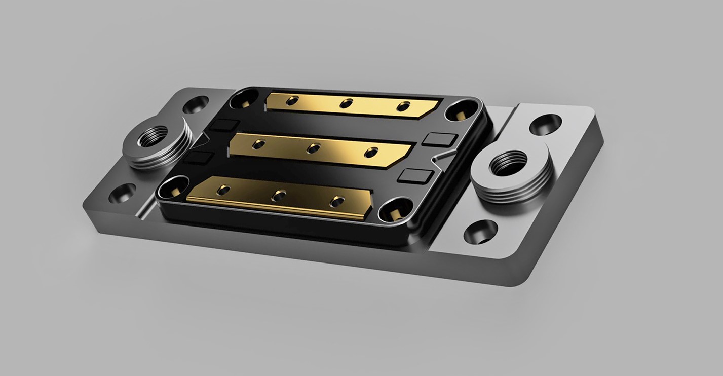
In another power CSP approach, designed to accommodate GaN or SiC power devices, the device is encased in a highly thermally conductive material. The 5mm x 6mm CSP eliminates the clip and wire interconnects of traditional discrete packages providing a direct source/drain/gate connection to the PCB. This CSP maximizes the source and drain connectivity area and eliminates lossy interconnects.
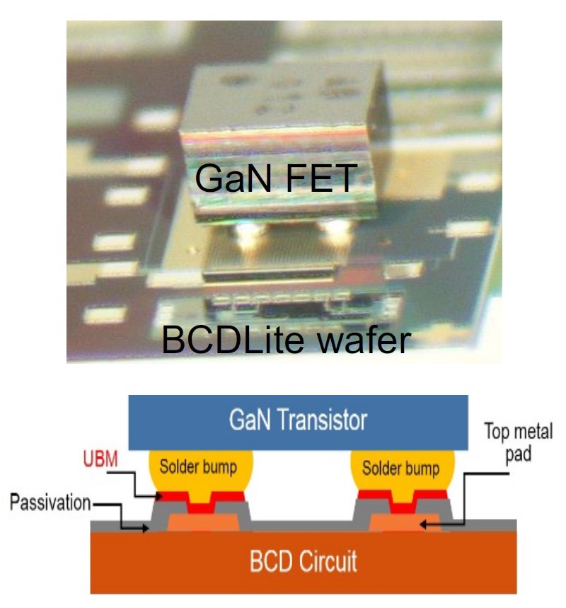
Heterogeneous packaging of GaN power transistors with integrated Si drivers can further reduce solution size and minimize performance-limiting parasitics. The close coupling between the gate driver and the power device minimizes ringing and overshoot. Wafer-level trimming can be used to adjust the controller to match the coupled GaN HEMT. And the matched coefficients of thermal expansion (CTEs) between the GaN-on-Si power device and the Si controller can improve temperature cycle reliability.
Power modules for high-power systems
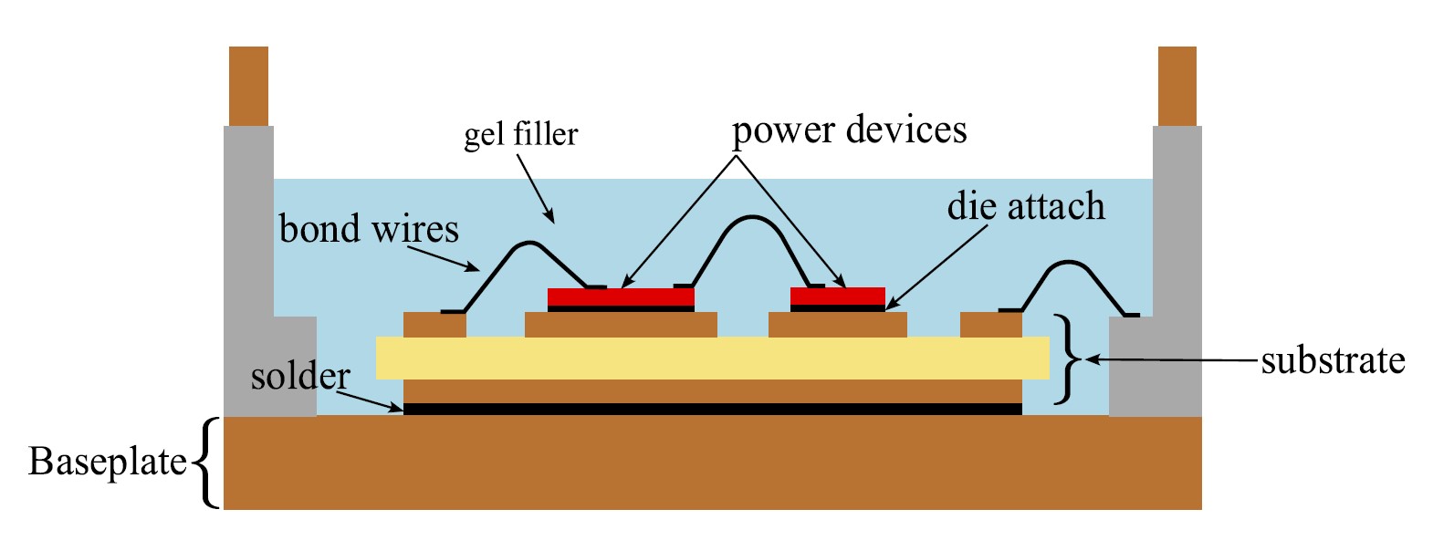
Traditional power modules for high-power converters used in automotive power converters, uninterruptible power supplies, motor drives, and industrial systems are designed to maximize thermal performance. Thermal management considerations are one of the primary challenges for emerging power PCB (also called PCB embedded) technology. The maximum operating temperature is limited due to the low glass transition temperature (Tg) and high CTE of conventional PCB materials compared with semiconductor materials. The embedded material in a power PCB can become more unstable at elevated temperatures than a traditional power module. That limits the power handling capability of the technology to a maximum of about 50kW, which hinders wide adoption in automotive applications. Advanced materials that are more thermally compatible with power devices must be developed to address that limitation. And those new materials have to be low cost.

Pressure-based power module assembly is also common. The joints in a press-pack power module are formed by pressure-based bonding, which is simpler and usually more reliable than the wire bonding, sintering, or soldering used in other power modules. And pressure-based bonding can be lower in cost. This type of packaging is mostly used in stationary applications and in systems that do not experience frequent thermal cycling. Automotive and transportation applications experience wide-range vibration and temperature cycling and are usually not good candidates for press-pack power modules.
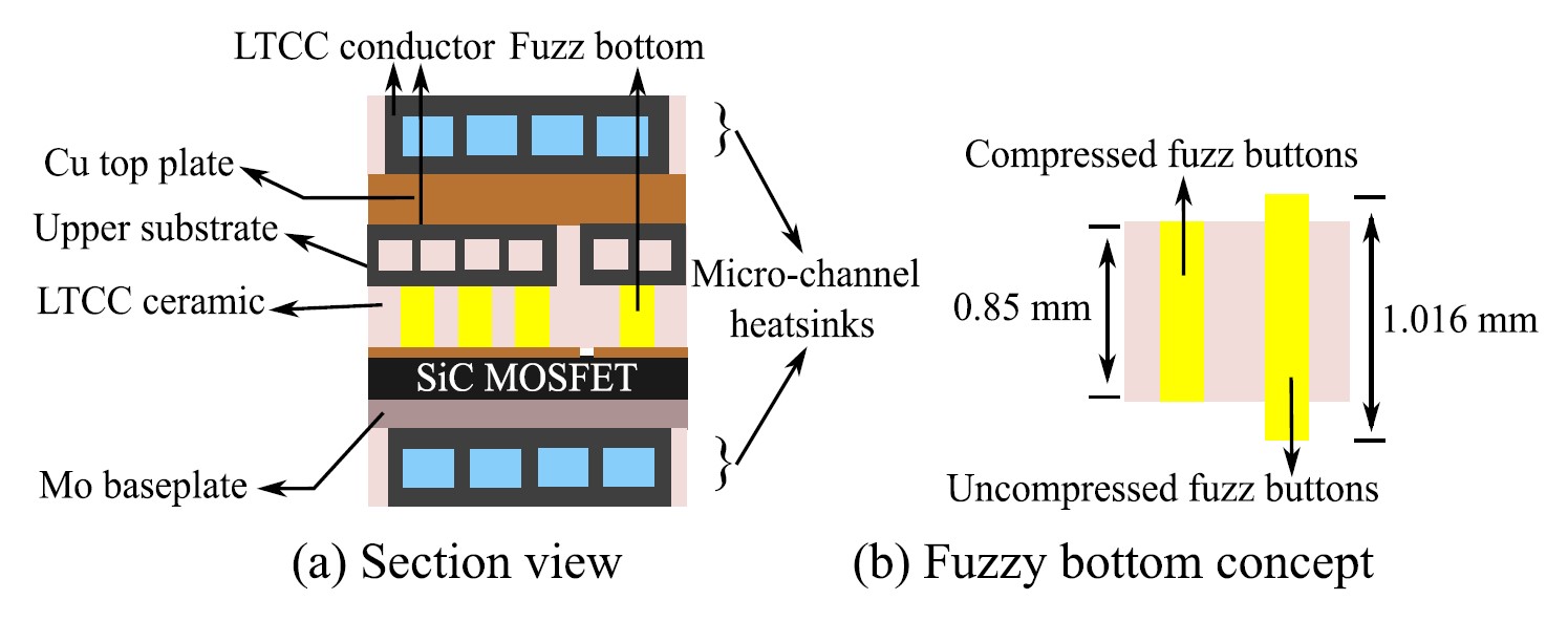
More advanced designs implement pressure-based connections using compressible interposers. In one case, a pressure contact interposer with a flexible structure (called a fuzzy bottom) is used in a stacked 3D package. The resulting structure has a larger tolerance for clamping pressure distribution and minimizes the skin effect when conducting current. Molybdenum (Mo) and copper (Cu) plates apply the clamping pressure.
In another configuration, a Beryllium (Be) / Cu spring is used to form the compression contact of the press-pack module. Be is one of the lightest metals and offers a combination of high strength, high fatigue resistance, and high thermal conductivity. But Be is much more expensive compared with Mo.
3D printing for power electronics
3D printing is being developed for various power conversion applications, including the production of electric vehicle (EV) inverters and battery chargers. 3D printing may be beneficial when using SiC or other wide bandgap devices whose performance cannot be easily maximized using conventional power module assembly techniques. 3D printing technologies are under development for EV power converters that overcome constraints relating to thermal management, electrical noise, and packaging volume while at the same time supporting high-volume and cost-effective manufacturing. As currently envisioned, 3D printing will be selectively combined with conventional power module packaging.
For example, a thermal base plate has been 3D printed with a complex internal lattice structure with walls less than 1mm thick, maximizing thermal performance while reducing weight. Combining the 3D printed thermal base plate with a conventionally designed power module package would result in 10% more current carrying capability, increasing the power density of the module.
3D printing also enables the fabrication of interconnects with optimized 3D geometries. Those interconnects will be used to move the gate drivers closer to the SiC power switches, reducing the solution size still further and reducing the loop inductance in the drive circuit, which will support higher switching frequencies, resulting in the use of smaller passive components and additional reductions in the size of the power converters. Finally, the more optimized drive design is expected to reduce EMI generation, contributing to simpler and smaller inverter designs.
3D printed power passives
The inevitable transition to WBG power devices will demand a change in current solutions for power electronics. Conventional methods and designs will not match the complexity, weight reduction, and level of integration of potential 3D solutions in power electronics. 3D printed magnetics, and other passive components, integrated cooling, and printed enclosures/structures will be required to satisfy thermal, mechanical, and volume requirements.
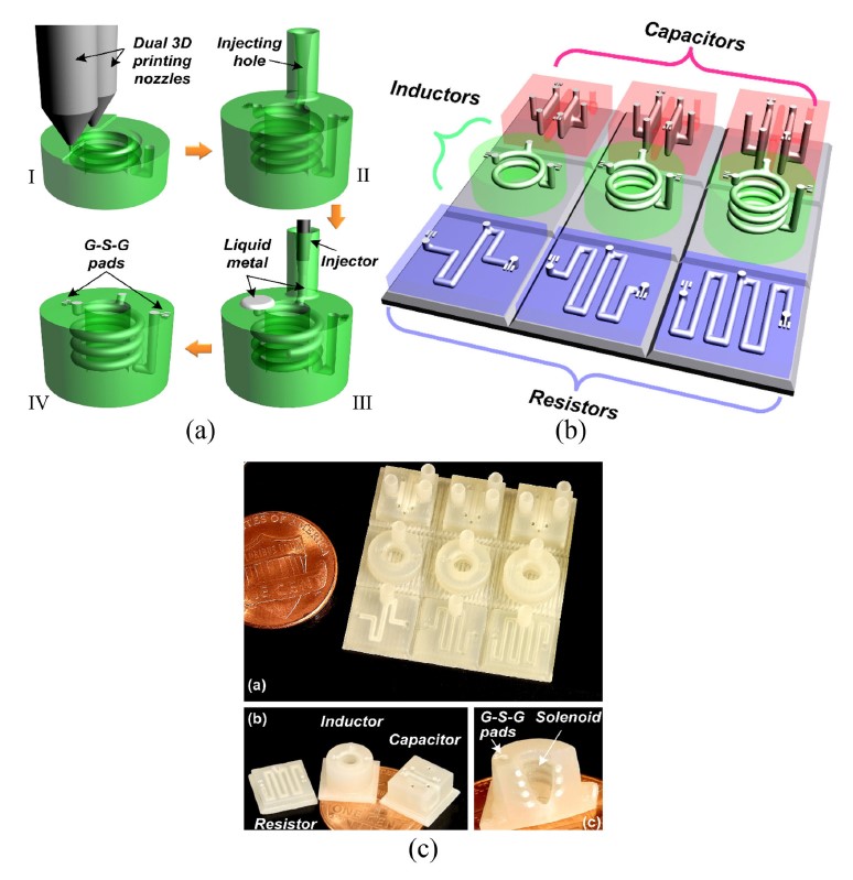
3D printing will enable the fabrication of customized inductors, resistors, and capacitors. It can produce good-quality capacitors and resistors. However, poor dimensional control of inductor coils (coil line width and spacing) results in non-uniformities that negatively impact the electrical properties. Higher resolution 3D printing is needed for inductor coil fabrication.
Today, the core and windings of magnetic components are manufactured separately, leading to performance limitations and physical size constraints. New geometries are being developed for 3D printed magnetic components that result in smaller component sizes and increased operating efficiency. But more advanced and precise 3D printing techniques are required and are under development. It’s no longer a question of whether 3D printing can successfully be implemented for power electronics applications but rather how it can be done cost-effectively at a mass production level.
Advanced thermal interface materials
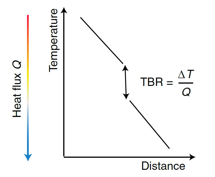
Achieving a combination of high thermal conductivity (HTC) with a low thermal boundary resistance (TBR is the resistance of an interface to thermal flow) near electronics junctions is key to high-performance thermal management systems. Diamond is considered the leading HTC material for high-performance power electronics cooling. Unfortunately, GaN-diamond interfaces have poor TBR, which reduces the application potential of diamonds for thermal management.
Using the Debye approximation method, the vibrational properties of materials are estimated using linear phonon dispersion. The maximum temperature of the highest phonon frequency is defined as the Debye temperature (ΘD). To achieve a low TBR, the two materials that make up the interface must have similar ΘD. The ΘD value of silicon, germanium, GaAs, and GaN, and most metals is below 700 K. Diamond has a ΘD over 2,000 K. Boron Arsenide (Bas) has a ΘD of about 700 K, making it a possibly superior alternative to diamond.
BAs substrates for thermal management can be heterogeneously integrated with metals and wide bandgap devices such as GaN transistors. GaN-on-BAs structures have a high thermal boundary conductance, and the powerful cooling performance of BAs exceeds that of diamonds. And, using AlGaN/GaN high-electron-mobility transistors (HEMTs) with BAs cooling substrates experience substantially lower hot-spot temperatures than diamond-based solutions. That makes BAs a possible solution for cooling next-generation high-power RF systems. Unfortunately, like diamond, the synthesis of cubic BAs is challenging, and its single crystal forms usually have defects. Efforts are underway to develop commercially viable methods of BAs synthesis.
Summary
The trends in advanced power electronics packaging are heavily influenced by the adoption of GaN, SiC, and other WBG semiconductor technologies. Power electronics packaging for WBGs is already borrowing from and building on packaging developments in the broader electronics industry, including chip-scale packages and heterogeneous integration. Getting the maximum performance from those advanced WBG power devices will require a range of additional technology developments such as 3D printing and advanced thermal management materials. If you’re interested in reading more about 3D printed electronics, check out “3D printing for 5G systems” and “3D and 4D printed electronics.”
References
Automotive Power Module Packaging: Current Status and Future Trends, IEEE
Chip scale packaging, Efficient Power Conversion
Current and Potential Applications of Additive Manufacturing for Power Electronics, IEEE
Heterogeneous Integration of GaN and Silicon for Power Conversion, GlobalFoundries
Integration of boron arsenide cooling substrates into gallium nitride devices, UCLA & Nature Electronics
Using 3D printing to add efficiency to EV power electronics, Institute for Advanced Automotive Propulsion Systems
Conferences
3D Power Electronics Integration and Manufacturing (3D-PEIM) Symposium
International Power Supply-on-Chip (PwrSoC) Workshop
International Workshop on Integrated Power Packaging (IWIPP)

Leave a Reply