By Roger Allan, contributing writer
There’s good news for power supply system designers. Silicon-based power devices are making performance advances in diode, transistor, and field-effect transistor (FET) functions. But wide-bandgap semiconductor IC technologies like gallium nitride (GaN) and silicon carbide (SiC) are poised to grow rapidly, offering designers greater performance in a smaller package, making design decisions more challenging.
Higher operating voltages, higher operating frequencies (faster switching times), higher temperature tolerances, and lower power dissipation than conventional silicon-based devices like diodes, transistors and field-effect transistors (FETs) are the hallmarks of GaN and SiC power ICs. Wideband gap (WBG) devices are those that offer higher voltage electronic gaps that are greater than 1 electron volt (eV). Silicon has a bandgap of 1.1 eV whereas SiC has a bandgap of 3.3 eV and GaN has a bandgap of 3.4 eV.
As part of its efforts to increase energy efficiency and double U.S. energy production by 2030, the Dept. of Energy (DoE) has awarded $22 million for WBG semiconductor IC developments. The aim is to merge WGB IC technology with advancements in driving megawatt motors for large-scale power generation and applications. The goal is to increase energy efficiency and decrease energy consumption of high-energy consuming industries, homes, fossil fuels and next-generation electric machines.
Silicon-based power IC technologies are limited by the inability of silicon to handle higher operating voltages, temperatures, and frequencies. The one advantage they have is a lower cost since they’re manufactured using conventional silicon processing steps.
Nevertheless, silicon-based power ICs are making their own performance advances in the form of advanced field-effect transistors (FETs) like high-electron-mobility transistors (HEMTs) and advanced MOSFETs that make use of insulated-gate bipolar transistors (IGBTs). IGBTs are presently the workhorses of the power electronics industry.
IGBTs continue to post advantages with higher performance attributes of high-speed switching, smaller size, and lower cost. An IGBT combines the simple gate-drive characteristics of a MOSFET with the high-current and low-saturation-voltage capability of a bipolar transistor.
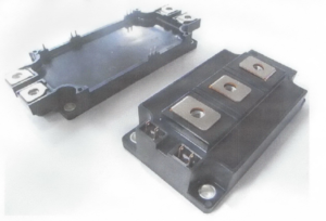
Recent IGBT market introductions include the 7th-generation low-loss T series of 650-V NX IGBTs from Powerex with higher efficiency levels in standard low-profile packages (Figure 1).

Powerex claims that they offer the best-in-class thermal impedance and very low losses. Built on the company’s CSTBT (carrier-stored trench gate bipolar transistor), the IGBTs find applications in 230-V AC motor drives, wind, and photovoltaic inverters, uninterruptable power supplies (UPSs), and medical equipment. The technology relies on optimizing the N+ emitter layer, the P+ diffusion layer, and the gate oxide thickness of the NPN transistor it uses in the IGBT to reducing the parasitic actions of the transistor and increasing operating temperatures up to 200° any thermal runaway and turn-off failures.
The new 1.2-kV M series IGBTs from STMicroelectronics feature advanced trench-gate field-stop technology to save energy and increase reliability in solar inverters, welding equipment, UPSs, and industrial motor drivers. They operate up to 20 kHz and up to 175°C.
IXYS Corp. uses its Ultra Junction technology to deliver a power IC figure of merit better than the state of the art according to Dr. Nathan Zommer, its CEO, and founder. These 650-V devices handle currents from 2 to 120 A, and feature an RDSon as low as 24 mΩ. “With the combination of reduced on-resistance and improved switching and thermal performance, these devices offer the best cost performance to our customers, even better than SiC MOSFETs, especially in ruggedness and reliability.”
Silicon MOSFETs Getting Better
Conventional silicon-based MOSFETs are finding room for designers to make the usual tradeoffs in smaller size, efficiency, lower switching speeds, power density and component count. Recent examples include the STMicroelectronics’ StripFET F7 devices that deliver the highest energy efficiency synchronous rectification. This allows the use of fewer parallel devices for a desired maximum current which helps increase power density and lowers component count.
STMicroelectronics has redefined power-conversion efficiency with new technology and packaging in its MDMesh DM-2 n-channel power MOSFETs with integrated fast-recovery diodes and a 650-V breakdown. It finds applications in low-voltage power supplies for computers, telecom networks, and industrial and consumer devices.
IXYS also offers 650-V X-2 class power MOSFETs with fast-recovery diodes made on its Ultra Junction process. With an on-resistance of 17 mΩ and current ratings from 22A up to 150 A, they’re optimized for soft-switching resonant-mode power-conversion applications.
For tight-space applications, Diodes Inc. offers the 100 V DMHC10H170SF dual n- and p-channel MOSFET in a tiny DFN5045 (5 by 4.5 mm). It’s aimed at applications that require multiple devices, such as in an array of ultrasonic transducers found industrial inspection systems or marine sonar equipment.
Infineon Technologies, which recently purchased International Rectifier Corp, offers the StrongIRFET DirectFETs which claim to deliver the highest energy efficiency in space-constrained applications like power tools and E-bikes (figure 2).

GaN Power ICs are Here
A WBG technology like GaN on silicon substrates is beginning to bear fruit and may open the door for power ICs over the next few years. Many GaN-based devices with performance improvements are coming out of the lab, and many like diodes, transistors, and FETs are appearing on the market.
A 900-V/32-A MOSFET platform, the first in the industry, is available from Cree Inc. The C3M0065090J is optimized for high-frequency power electronics applications like renewable energy inverters, electric vehicle (EV) charging, and 3-phase industrial power supplies. It has 65 mΩ of on-resistance and is available in TO-247-3, TO-220-3 and D2Pak-7L SMT packages.
Military, automotive and industrial applications can also make use of GaN FETs from Efficient Power Conversion Corp. like the EPC2040. Optimized for pulsed applications, the tiny die (0.85 by 1.2 mm) features a VDS of 15 V, an RDS(on) of 28 mΩ, an ID of 3.4, and a pulsed ID of 28 A.
Panasonic Corp. claims it has developed GaN diodes that can not only operate at high currents four times greater than SiC ones, but also has a low threshold voltage. The diodes can handle 7.6 kA/cm2, require a low turn-on voltage of 0.8 V, and feature a low on resistance of just 1.3Ω/cm2. To achieve this performance, Panasonic used a hybrid structure of GaN diodes with a trenched p-GaN layer which can be removed selectively during processing by an n-type layer.
Prototype samples of a GaN FET in modular form like the 80-V 10-A LM5200 are available from Texas Instruments. Aimed at applications that require increased power density and efficiency in space-constrained high-frequency industrial and telecom applications, the module contains two GaN FETs in a half-bridge configuration and a high-frequency driver all housed in a quad no-lead (QFN) package.
Automotive electronics supplier Hella, in collaboration with Canada-based GaN Systems, and charging technology researchers at Kettering University’s Advanced Power Electronics Lab, developed an industry-leading EV charger. Using GS66516T, the Level-2 EV chargers showed prototypes with efficiencies of more than 97%, at an unprecedented 2.6 kW/l.

SiC Forging Ahead
Wolfspeed Inc. recently offered samples of its C2M1000170J that handles 1.7 kV. Optimized for this rating in a SMIT package, it has an avalanche rating greater than 1.8 kV and an RDS(on) of 1 Ω. Its small footprint with a wide creepage distance of 7 mm between the source and drain terminals suits it for auxiliary power supplies with high-power inverters, uninterruptable power supply (UPS) equipment, wind-energy converters, and traction power systems.
One of the newest SiC MOSFETs is the SCT20N120 from STMicroelectronics (figure 4).

This 1.2-kV device has an RDS(on) of 290 mΩ all the way up to the 200°C maximum operating junction temperature. Housed in STMicroelectronics’ HiP227 package that’s compatible with the industry standard TO-247 power package, it permits switching frequencies 3X higher than similarly rated silicon IGBTs.

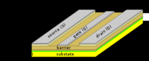
An HEMT transistor can operate at higher frequencies (millimeter waves) than ordinary transistors, for mobile phone communications, satellite TV receivers, voltage converters and radar equipment. (Source: Wikipedia).
Such devices incorporate a junction between two materials with different as the channel instead of a doped region (as is the case for MOSFETs). HEMT transistors can operate at higher frequencies (millimeter wave frequencies) than ordinary transistors, for mobile phone communications, satellite TV receivers, voltage converters and radar equipment.
The newest Cree company, Wolfspeed Inc., has unveiled plastic-packaged CGHV27060MP GaN HEMT FETs for low-cost 50-V 60-W applications. They’re supplied in 4.5-mm by 6.5- mm surface-mount (SMT) packages to suit long-term evolution (LTE) phone, cell-based station, radar, public-safety radio, and other communications applications.
Wolfspeed is a leading supplier of GaN HEMTs and monolithic microwave ICs (MMICs) grown on SiC wafers for commercial and military markets. They feature a combined RF output of 1.3 GW of power and a failure in time (FIT) rate of 5 per billion device hours.
The unmatched and recent 50-V 50-W GaN transistor from Cree uses an HEMT structure and provides high-performance broadband solutions for RF and microwave applications up to 4 GHz, including narrow-band UHF, L-band, S-band, and multi-octave bandwidth amplifiers. The CGHV40050 exhibits high-efficiency, wide-bandwidth, and high-gain performance.
GaN Systems Inc. is marketing the G S66540C 650-V 100-A GaN transistor based on the company’s proprietary Island Technology die design that produces devices with fast switching speeds of 100 V/ns with very low thermal losses. Part of the company’s portfolio of enhancement-mode HEMT family, it makes use of a patented GaNPX packaging and Drive Assist technology which together with the Island Technology provides GaN HEMTs with a 45 times improvement in switching and conduction performance over silicon MOSFETs and IGBTs.
GaN or SiC?
In the short term over the next 4-5 years, GaN will fulfill many power IC applications in the 600-V to 1.2-kV range. Two voltage options are being targeted, 600 V and 1.2 kV. Present applications include solar inverters, electric and hybrid electric vehicles (EVs and HEVs), uninterruptable power supplies (UPSs), communications, and RF solid-state power amplifiers.
However, in the longer term, SiC IC power technology is poised to gain some ground, particularly for applications that require very high temperatures and extreme ruggedness, very low switching losses, rolling-stock uses like trains, transportation, very high voltages of 2 kV or more, and geophysical applications like oil and gas drilling. Some companies have already introduced SiC MOSFETs that can reduce switching losses by more than 70% compared with IGBT MOSFETs.
According to research by HIS Inc., the GaN and SiC power market will exceed $2.5 billion by 2023. “While end users now prefer normally-off SiC MOSFETs, SiC JFETs and BJTs look likely to remain specialized niche products,” says Richard Eden, an IHS senior analyst.
Analyst Pallavi Madakasira, leader of the study “Breaking Down the GaN Electronics Market” at Lux Research in the U.S. points out that GaN on silicon substrates offer performance improvements over other approaches like GaN on GaN substrates and GaN on SiC substrates, the latter two which “will limit their adoption.” She sees the transportation and renewable energy/smart-grid sectors as key markets, reaching sales of $350 and $380 million, respectively. She forecasts the overall GaN IC power-conversion market to grow to $1.1 billion by 2024.
A similar assessment of the growth of GaN power IC technology is made by France’s Yole Développment in conjunction with KnowMade, a Yole partner, based on intellectual property (IP) dynamics. “The future of GaN devices also depends on the growing global patent landscape and coming mergers and acquisitions” explains Nicolas Baron CEO of KnowMade (figure 6).

Yole has already forecasted dynamic growth for both GaN and SiC power devices. It sees competition for applications from both technologies setting up a question mark of “how will GaN and SiC technologies cohabitate?” In Yole’s “nominal” market scenario, it estimates that the market size for GaN power ICs will be $303 million by 2020.


Leave a Reply