Side-by-side performance comparisons can show where silicon-carbide excels in PV installations.
Steven Shackell • onsemi
According to the International Energy Agency, solar power (PV) installations are on track to reach an installed capacity of 3,300 TWh by 2030, a yearly growth rate of 15% from 2019. Installations will be a mix of micro, mini and utility-scale, but all with similar PV technology: Cells will be connected in series for high, usable voltages and in parallel for higher power.
A trend is to increase voltages with strings of panels to gain the advantage of proportionally lower current, producing less power loss in connections and cabling. Typical nominal panel installation voltages are around 500 to 1,000 V but 1,500 V is predicted to eventually become more common.
Rather than using a single central inverter, each string will often have its own relatively low-power inverter for scalability, economy and fault tolerance. Typically, the PV voltage is boosted to a regulated dc value suitable for input to a dc-ac conversion stage. And a Maximum Power Point Tracking (MPPT) controller optimizes the load on the panel for best energy efficiency. The boost dc-dc converter and inverter are high-efficiency switching circuits, and the semiconductors employed can be of various technologies.
Insulated Gate Bipolar Transistors (IGBTs) have dominated high power dc-dc and ac-dc conversion, but new wide band-gap (WBG) semiconductors such as silicon carbide (SiC) MOSFETs are having an impact. Their ratings that compete into the tens-of-kilowatts range and even higher when paralleled. Both technologies are available not only as individual devices in common packages, such as the TO-247, but also as power integrated modules (PIMs). A PIM is basically an industry standard housing that holds several switches, sometimes including diodes and even drivers and protection circuitry. With PIMs, a single package can provide a complete power stage for converter and inverter functions.
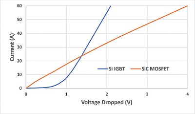
IGBTs and SiC MOSFETs differ markedly in several respects. IGBTs are restricted to low frequencies because of their dynamic losses but drop a nominally constant saturation voltage when conducting. This behavior leads to a power loss simply proportional to current. SiC MOSFETs, in contrast, can switch at hundreds of kilohertz with low dynamic loss but exhibit a nominally constant resistance when conducting. This behavior leads to a power loss proportional to the square of current, clearly an increasing disadvantage as power throughput rises.
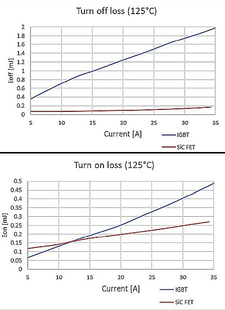
Dynamic losses are frequency-dependent. If IGBTs and SiC MOSFETs are compared at around 20 to 30 A switching at the same low frequency, say 16 kHz, conduction losses are similar but dynamic losses are quite different. Consider two sources of switching loss, turn-on and turn-off energy Eon and Eoff respectively. IGBTs have a lower turn-on loss at low current, but there is a crossover point; the Eon of both device types is at around one-quarter of the conduction losses, a little worse for IGBTs but not a large absolute value. However, Eoff is much higher with IGBTs because of ‘tail’ current. These are minority carriers that must be swept out of the device N-drift region on turn-off, producing transient power dissipation. There is around a factor-of-ten difference for Eoff between the device types.
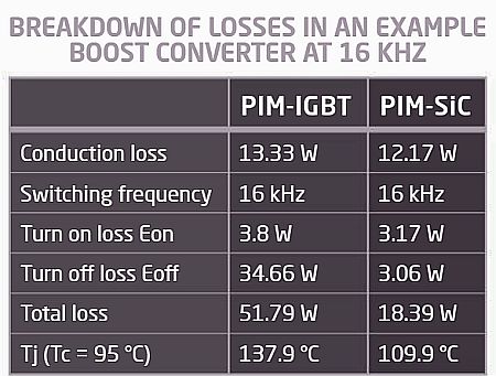 It is useful to consider the differences between a practical PV boost converter based on a PIM-IGBT vs one using a PIM-SiC device. A nearby table summarizes the two with an input of 500 V, 25 A and an output of 800 Vdc, running at 16 kHz and 95°C case temperature. There is a clear overall power saving with SiC which exhibits a total loss of around a third that of the IGBT circuit and a lower junction temperature for higher reliability.
 Besides energy savings, the benefit of better efficiency with SiC includes reduced size and heatsinking, a lower rise in temperature for the same heatsinking or, alternatively, higher power throughput for the same heatsinking and temperature rise. In addition, it is worth investigating the high-frequency capability of SiC. Though the SiC devices have a higher junction temperature, as WBG devices, they typically are rated for 25°C higher operation than silicon. SiC MOSFETs still show a significant efficiency gain over IGBTs and a little over half the losses. However, operation at a higher frequency also allows use of a boost inductor physically smaller by around a factor of three with consequential cost and weight savings. Additionally, there can be less EMI filtering at the fundamental frequency and low harmonics with further savings.
But SiC MOSFETs do have fast rising and falling edges. So high-frequency filtering must be considered carefully to meet emissions standards.
Losses are not the only differences between IGBTs and SiC MOSFETs. For example, MOSFETs contain a body diode which is absent in IGBTs. The body diode can be useful in conversion stages that require reverse or ‘third quadrant’ conduction in the switch. The SiC MOSFET body diode can provide the conduction although its forward voltage drop is relatively high. So an extra parallel diode must be added when using IGBTs this way.
Thus there is a point where benefits from the use of SiC at a higher frequency are substantial enough to outweigh their additional PIM unit cost. SiC MOSFET on-resistance declines with every new generation of devices, so the benefit cross-over point continually rises to higher power levels
SiC design considerations
The gate drive for IGBTs and SiC MOSFETs may seem nominally similar. But the on-drive for the SiC device is more critical for lowest conduction losses. It must be as close as practical to the absolute maximum of typically 25 V. For this reason, 20 V is often used, giving some safety margin. Both device types are nominally off with a 0-V gate drive, but both are often driven negative by a few volts. This gives smaller Eoff, less gate-source ringing on turn-off, and helps prevent ‘phantom turn-on’ which can result from spikes from any source or emitter inductance common to the gate drive loop.
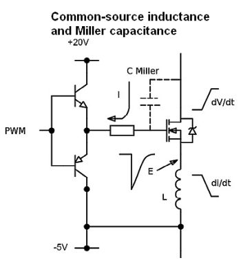
Any device Miller (drain to gate) capacitance can also tend to spuriously turn devices on with high drain or collector voltage edge rates (dV/dt). Again, the negative gate drive helps to avoid problems.
SiC MOSFETs have much higher dV/dt and di/dt than IGBTs. Thus high-frequency layout techniques with careful decoupling are necessary to avoid unreliable operation and excessive EMI. Drivers must be close to the SiC MOSFET PIM. and any available Kelvin connection to the MOSFET source should be used as the driver return, to avoid common inductance.
It can be difficult to accurately measure the dynamic performance of SiC MOSFET PIMs due to the fast edge rates. Typically test equipment should have at least 300 MHz bandwidth and high-frequency measurement techniques are in order. Voltage probes should be connected with a minimum ground loop and current monitored with high-performance sensors such as Rogowski coils.
Making the switch from IGBTs to SiC MOSFETs is a net system benefit at increasing power levels, with PIMs providing an easy avenue. Those familiar with using IGBTs, however, should be aware that a simple swap-out will not give good results – optimum performance requires a re-evaluation of gate drive arrangements, layout and EMI filtering.




Leave a Reply