The smartphone migration from 4G to 5G brings mmWave bands with wider bandwidths, speedier data rates, and higher production test costs. These higher costs for equipment and operations in high-volume manufacturing (HVM) parts force manufacturers to rethink the economics of automated test equipment (ATE). The insights gained from analyzing test costs may even set the bar for future generations of devices, depending on the lessons learned in this current ramp. At the core of this topic is the ATE financial analysis for mmWave technology commercialization. Such analysis will directly affect how much test capacity a production facility needs and how many test sites minimize total costs.
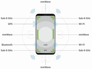
Figure 1 shows a typical 5G smartphone. The number of wireless links that fit in today’s devices, which enable applications that use primary navigation, connectivity, and cellular technologies, is an impressive engineering feat. Equally impressive are the other technologies, including display, digital, and battery.
RF Architecture
Figure 2 shows the evolution in signal distribution within the 5G smartphone’s front-end, segmented between sub-6 GHz and mmWave. Sub-6 GHz frequency bands have low, medium, and large links (in bandwidth). Even the largest pales in comparison to the massive links possible with mmWave technology.
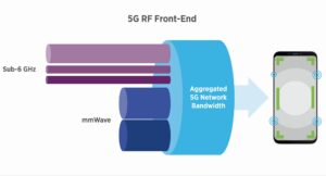
Figure 2. The 5G RF front-end segments in two categories: Sub-6 GHz and mmWave. In general, the Sub-6 GHz links offer useful data rates while mmWave links are 10x greater in data rate capabilities.
While many engineers understand sub-6 GHz, the mmWave links are new to 5G and require closer inspection to understand the technology and economics of commercialization.
Figure 3 shows a detailed overview of the RF architecture that enables these 5G links [Ref. 1]. Note the added mmWave complexity in the integration of the modem, 5G-IF link, and mmWave transceiver, which includes the beamforming antenna. The mmWave antenna requires strategic placement to minimize blockage from hands; the 5G-IF feature supports the link budget for optimal signal quality.
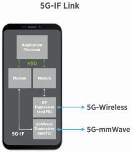
Figure 3. This RF architecture reveals the key chips and features that enable mmWave technology within the 5G smartphone, including the high-speed digital (HSD) connections to the front-end (FE). In this way, RF to bits is woven into the RF architecture.
Comparing RF architectures, the sub-6 GHz band is a baseline and the mmWave link introduces a new intermediate prerequisite, 5G-IF, for 8 GHz to 20 GHz testing. In doing so, the test plan complexity increases dramatically (test duration, tester resources, methodologies, and calibration to name a few). The additive complexity is related to the sub-6 GHz to baseband (RF to bits/analog), whereas mmWave is RF to an intermediate frequency (IF) before ultimately arriving at baseband. To complicate matters, the mmWave links are deployed in multiple places within the 5G smartphone for spatial diversity.
5G smartphone ramp
Unfortunately, mmWave links increase the amount of test required and therefore have a dramatic effect on the economics. At the time of publishing, the 5G smartphone is offered in two high-level configurations: economy tier and premium tier. The premium tier includes mmWave. Figure 4 shows a 5G smartphone forecast developed by Teradyne, which estimates that 1.2 billion units per year will ship by 2025. The RF architecture flexibly supports both the economy and premium configurations and can likely scale to unit shipment levels consistent with 4G smartphones. Remember that the proportion of phones with mmWave links will increase over time.
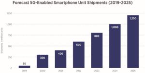
Figure 4. A 5G smartphone forecast developed by Teradyne quantifies the amount of semiconductor content (i.e., chips) that fuels the economics for mmWave commercialization. Today, only premium smartphones include mmWave while the rest are economical configurations with sub-6 GHz bands only.
Adding mmWave to a smartphone increases manufacturing costs; the challenge is how to minimize the economic impact. There are many proven techniques, such as reducing test time, but these lack the impact to overcome mmWave expenses. This new silicon will benefit most from considering increasing site counts. As a baseline, today’s HVM has standardized on a given number of sites (e.g., x4, or x8). The next section explores the financial implications of increasing sites.
Tester fleet economics
The economics of deploying a tester fleet is well known so the focus is on a financial comparison of scenarios involving the number of sites [Ref. 2]. Predictably, this single configuration choice has the largest effect on the overall economics, which is why you should give it the most consideration in ramping new silicon.
As a quick introduction, these high-level economic indicators are as follows:
- Capital equipment expenses (CapEx). This is the initial expense associated with obtaining the necessary test equipment, (e.g., tester and handlers). CapEx usually depreciates over a five-year period corresponding to the lifetime of equipment.
- Operating expenses (OpEx). This is the yearly operating expenses associated with the operation of the equipment, which can include the consumables that customize testers for a specific device under test (DUT).
- Total cost of test (CoT). The sum of all fleet expenses over a typical lifecycle, both CapEx and OpEx, divided by units shipped.
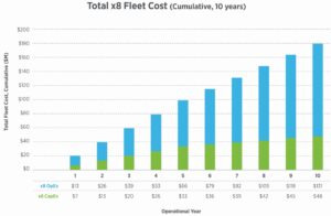
Figure 5. Cumulative fleet cost over time shows more OpEx than CapEx contribution to economics. Note the difference in trajectories suggests that optimizing OpEx as a priority will have more impact on total cost of test.
For the financial comparison in Figures 5 and 6, we consider the final test of a packaged RF transceiver device (i.e., not-wafer although, the economics are similar). The approach is high-level to assess macro insights. As a typical user scenario, the units per year are proportional to 5G smartphone unit shipments, where the mmWave variant has x3 or x4 links. For purposes of this financial analysis, we will target 100 M units per year with a nominal test duration of 30 sec per device. The fleet depreciation period is five years while the typical lifetime is 10 years. A side-by-side comparison of x8 versus x16 sites should produce recommendations for how to configure the tester fleet for new silicon ramps. Actual results and configuration vary so apply the following takeaways on a conceptual basis.
Figure 5 shows the baseline fleet costs for x8 sites where cumulative results are calculated over time. The yearly breakdown into OpEx (blue) and CapEx (green) illustrates that OpEx has the greatest impact on total CoT beginning in the first year and establishes the trajectory for subsequent years. In contrast, CapEx is more constrained due to the depreciated nature of that expense.
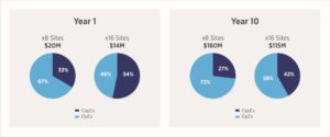
Figure 6. Cumulative comparison of x8 versus x16 sites in terms of CapEx/OpEx breakdown. Note lower total expenses in x16 scenario. The takeaway is a redistribution of expenses occurs with greater site count: OpEx expenses dominate total CoT, and the reduction in OpEx is proportional to fewer testers, handlers, and consumables.
Similarly in Figure 6, cumulative fleet calculations for x8 and x16 cases enable a side-by-side comparison.
At the end of year 10, the total unit shipments are 1 billion (100M/year times 10 years), so the total CoT calculation is straightforward:
x8 sites produces total CoT of $0.18 at a total cost of $180 M (CapEx/OpEx ratio of 27%/73%).
- x16 sites produces total CoT of $0.11 at a total cost of $115M (CapEx/OpEx ratio of 42%/58%), a 39% reduction in total CoT.
In this comparison, lifetime savings of $65 M are possible by migrating to x16 sites.
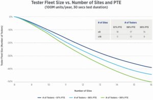
Figure 7. The tester fleet size for unit shipments of 100M/year (and test duration of 30 secs/DUT). Compared to x8 sites, increasing sites to x16 has the net effect of reducing the number of testers from x18 to x9, which has a dramatic effect on OpEx.
In Figure 7, the number of testers in a fleet is over 38% fewer when comparing x8 to x16 sites. The concept of parallel test efficiency (PTE) is important to introduce as a mechanism for quantifying the independence of parallel test duration. Ideally, 100% translates to complete independence. Usually, PTE is in the 97% to 99% range as shown in Figure 7 trace overlays. The key takeaway is each site needs dedicated tester resources to deliver the economic benefits of more sites. In addition, this PTE insight demonstrates the impact is greater as site counts increase; in fact, at x16 sites, a 1% PTE delta equates to a ~10% fleet size delta.
At the next level of granularity, the economic results in Figure 8 overlay units per hour (UPH) and CoT for sites from x8 to x16 and considers the impact of PTE. Note how the PTE has a greater effect with the greater number of sites; in fact, at x16 sites, a 1% PTE delta equates to a ~20% UPH delta.
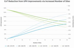
Figure 8. As a result of reducing the number of testers, the CoT exhibits the reduction characteristics shown above, which is proportional to the units per hours (UPH) improvement that results from higher site counts.
Conclusion
The complexity of adding multiple mmWave links to the 5G smartphone affects the RF architecture in such a way that is similar to, but proportionately higher, than existing Sub-6 GHz implementation. Thus, the economics for production testing are similar and predict a prohibitively expensive increase in total CoT for new silicon. By increasing sites, the potential to offset some of this additive mmWave expense is possible and may even accelerate the commercialization of mmWave technology.
Increasing test site counts will have the most dramatic impact on fleet economics and total CoT. The impact is related to reducing the number of testers and, in doing so, proportionally reducing the OpEx necessary for HVM (which dominates total CoT). It may be counterintuitive, but greater CapEx that produces higher units per hour is highly desirable for the dramatic reduction in testers, handlers, and consumables, which has a corresponding reduction in OpEx, especially in the context of lifetime calculations.
In a new silicon perspective, these results reveal that test engineers should prioritize their total CoT activities as follows:
- Minimize OpEx with focus on UPH, including consideration of greatest parallel test efficiency (PTE).
- Minimize test duration.
- Minimize CapEx.
This holistic and lifetime approach to HVM planning optimally configures the tester fleet to deliver the best economics.
The smartphone follows the 18-month cadence of Moore’s Law. Moreover, new silicon will continue to evolve in ways that deliver enhanced experiences to consumers, as seen with the emergence of mmWave technology. Sustaining a growth trajectory is a cyclical process in the relentless pursuit of cost reductions. ATE parallelism and efficiency are vital mechanisms fueling growth in the HVM semiconductor ecosystem.
References
1. Hurtarte, Jorge S., “Test Challenges and Solutions for Testing Wi-Fi 6E, UWB and 5G NR IF Devices in the 3-12 GHz Range“.
2. Kramer, Randy, “Test strategy implications on cost of test,” Evaluation Engineering, Jan. 25, 2018.
 David Vondran has a B.S. degree in electrical engineering from California State Polytechnic University, Pomona. He has held engineering and marketing positions at Rockwell International, Watkins-Johnson, Pacific Monolithics, California Microwave, Anritsu, OML, LitePoint, Advantest, and Astronics Test Systems. David is currently the wireless product manager at Teradyne.
Rob Messier has a B.S. degree in electrical engineering from Northeastern University. He is currently the wireless applications specialist at Teradyne where he engineers commercialization ramps on emerging technology, including mmWave applications. Rob has been with Teradyne for more than 25 years, during which time he has contributed significantly to the wireless semiconductor ecosystem.

