Choosing an op amp and getting the best out of it involves some understanding of what is inside the chip, particularly the input stage.
Simple bipolar input stage
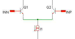
A conventional bipolar opamp will usually have a long-tailed-pair with two NPN or PNP input transistors as shown below. This explains the limited working range of a typical opamp – the inputs must be at a high enough voltage to keep the emitters of the long-tailed-pair high enough so the current source still behaves like a current source. Similarly, the bases cannot go too high otherwise the load for the long-tailed-pair will stop functioning correctly, although there are ways round that to allow the inputs to work very close to one voltage supply rail.

There are still a lot of bipolar opamps around, particularly for high-speed applications.
Input bias current cancellation
This was covered in detail in an earlier blog. It involves arranging some extra transistors to provide the base bias current required by the bipolar transistors instead of the current coming from your design. It will never be perfect but will reduce the input bias current by at least an order of magnitude.
PMOS (or NMOS) input stage
In place of NPN or PNP transistors, you can use NMOS or PMOS respectively so a CMOS process can be used. A similar issue with input voltage range will exist, as for bipolar input stages although with careful opamp design you can make the input voltage range extend to one of the supply rails. While this can also be done with bipolar designs, often your choice of transistor is more restricted in bipolar design so it can be tricky to achieve.
Rail-to-rail input
With lower power supply voltages the loss of input voltage range due to the simple bipolar/MOSFET long-tailed-pair input stages is quite a nuisance so rail-to-rail input (and output) opamps have evolved. A couple of techniques are possible, the first being complementary input stages. You would combine a PMOS long-tailed-pair input stage with an NMOS input stage as shown below.
Q37 and Q32 are the NMOS inputs and Q14/Q15 the PMOS inputs. The loads for these transistors are more complex as there are two separate loads (one each for the NMOS & PMOS) and the outputs need combining. One problem with this sort of design is trying to ensure a consistent performance at any common mode input voltage. At high input voltages you will only be using the NMOS inputs – the PMOS ones will be ineffective. At low input voltages only the PMOS inputs will be effective and in between you will have the combined effect of the two. This means that the open loop gain and gain bandwidth product can vary depending on the input voltage. This is not ideal and careful design is required to minimize the effect.
Another approach to achieving a rail-to-rail input is simply to boost one of the supply voltages. With a PMOS input stage a capacitive charge pump can create a voltage a little above the positive rail in order to supply the input current source. This can all be on-chip and has the advantage of a simpler opamp design with a more consistent performance with input common mode voltage changes.
JFET input
While a lot of new designs of opamp are CMOS there is still a place for JFET input opamps where low voltage and current noise are required. Bipolar opamps can have low voltage noise but if you have a high source resistance for designs such as photodiode amplifiers and charge amplifiers you will want near zero input bias current and low current noise. A JFET input opamp design looks very much like a bipolar one but with a JFET long-tailed-pair instead of bipolar one. The JFETs would usually only be used for the two input transistors. While devices such as the LF411 and TL081 from Texas Instruments are JFET input, they have quite high voltage noise. Devices such as the Analog Devices AD743 and AD745 combine the low voltage noise of a bipolar opamp with the low current noise of a JFET to give the best of both worlds. They do have a limited input common mode voltage range, however.
BiCMOS
BiCMOS designs are another attempt to improve the performance of a pure CMOS opamp by including a few bipolar transistors in the front end long-tailed-pair. This can result in higher gain bandwidth product than a pure CMOS design, depending on the design objective and how the design is implemented. However, they seem less common now, possibly because the performance of pure CMOS opamps has improved considerably and BiCMOS processes cost more than pure CMOS processes.


Leave a Reply