By Michael Score, Texas Instruments
Switching power supplies are used in almost every end-equipment that needs a long battery life, low heat generation, or to meet ENERGY STAR® guidelines. When designing a switching power supply, it is difficult to decide which output capacitor type to use.
Electrolytic capacitors have high equivalent series resistance (ESR), making power loss high and transient response too poor for use with tough load-response requirements. However, electrolytic capacitors have stable capacitance with high bias voltage and are inexpensive. Ceramic capacitors have very low ESR, but capacitance is reduced greatly with high bias voltage and can be expensive for large values. The effective capacitance of a ceramic capacitor can be less than half the rated capacitance in many buck converters.
Today’s buck regulators typically use just one type of output capacitor because it becomes too difficult to design with different capacitances and ESRs. This forces many designers to use more expensive capacitor types like polymer or tantalum that provide lower ESR than electrolytic, but not as low as ceramic. Now a stable design with mixed output capacitors can be prepared in minutes by using new design tools. To illustrate this concept, this article describes the design of a DC/DC supply with mixed output capacitors.
Causes of output variation under load
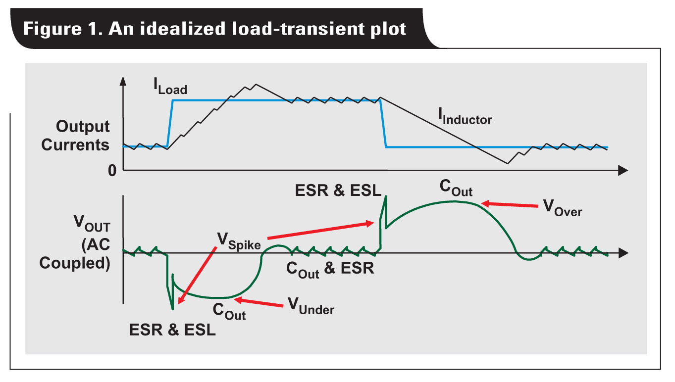
The first step is to understand what the output capacitor does in the system. Figure 1 shows idealized waveforms with contributions of output-capacitor characteristics and where they occur in a load-transient event.
The spikes at the load transients are primarily caused by equivalent series inductance (ESL) or impedance of the output cap at very high frequencies. Fixed inductor-current slopes cause the bulk of the transient-event disturbance in the inductor current to overshoot and undershoot.[1] Recovery from the load-step transient also causes overshoot and undershoot. Minimizing these lower frequency errors relies on energy stored in the output capacitor and the voltage-loop response time. So, it is important to have a wide loop bandwidth, low ESR, and enough output capacitance for adequate storage.
There are two primary factors for maintaining low-noise output under load: 1) how much overshoot and undershoot the regulator will have; and 2) how much ripple voltage occurs at the switching frequency. Peak overshoot/ undershoot is approximately the load-step current times the impedance of output capacitors at the loop crossover frequency (Equation 1). The equation emphasizes the importance of having low output-capacitor impedance at the loop crossover frequency (fC) to get low overshoot or undershoot. The loop crossover frequency is usually targeted to be one-tenth the switching frequency. A higher loop crossover frequency minimizes overshoot/undershoot.
VOVER/UNDER SHOOT ≈ D IOUT × ZOUT (fC) (1)
An approximation for output ripple voltage is the output capacitor’s impedance at the switching frequency times the peak-to-peak inductor current.
VRIPPLE ≈ IL(P-P) × ZOUT (fSW) (2)
Equation 2 shows that the output ripple voltage can be reduced by reducing the peak-to-peak inductor current, which is controlled by increasing the inductance value. However, there are drawbacks. A more effective way to minimize ripple is to reduce the output capacitor’s impedance at the switching frequency. The impedance used for ripple voltage is at a much higher frequency because the switching frequency is around ten times the loop crossover frequency.
To minimize ripple and overshoot voltage under load transients, the regulator requires a wide loop-crossover frequency. There should also be sufficient capacitance for energy storage and the impedance of the output capacitors should be low over frequency.
Output capacitors minimize output impedance
Ideally, the output capacitor would be very large for energy storage and have very low impedance at the loop crossover and switching frequencies. Polymer and tantalum capacitors come in large values with low ESR, but they are expensive and the ESR is still not as low as a ceramic capacitor. Electrolytic capacitors are very good for obtaining large capacitance values at a low cost, however, they have a larger ESR and ESL. This makes them unsuitable for output load-step performance.
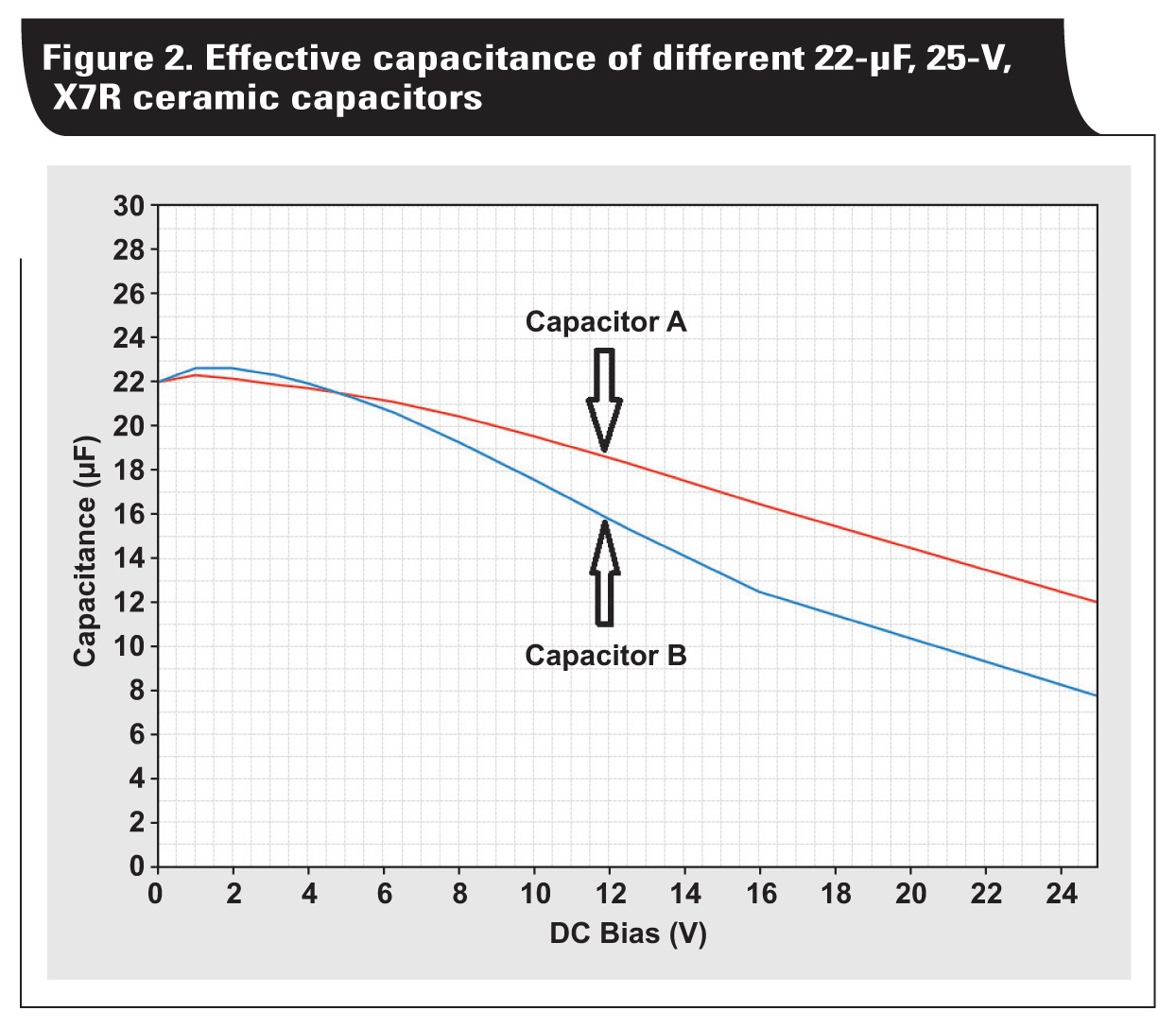
Ceramic capacitors have very low ESR and ESL that makes them great for transient performance, but they have limitations on capacitor size. Ceramic capacitor values of 22 µF and less are relatively inexpensive. The effective capacitance of ceramic capacitors decreases with bias voltage, which makes it more difficult to provide enough energy storage for large load steps. TDK SEAT software was used for the plot in Figure 2 to show the effect of VBIAS on effective capacitance. The two 22-µF-rated ceramic capacitors decrease to 19 µF and 16 µF with 12 V of bias voltage. Note that two 22-µF, 25-V, X7R capacitors from the same vendor have very different VBIAS curves, so be sure to check the actual VBIAS curve.
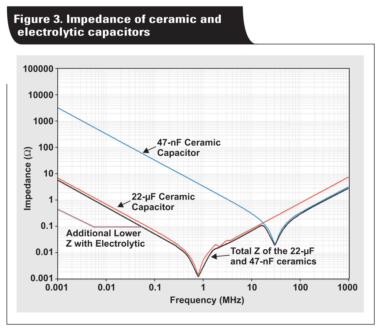
With the same software, Figure 3 shows the impedance of 22-µF and 47-nF ceramic capacitors versus frequency. The 22-µF capacitor has low impedance at 100 kHz and above, but it does not provide enough energy storage. The electrolytic capacitor can be paralleled with the 22-µF ceramic, allowing low impedance at frequencies less than 100 kHz. The electrolytic capacitor is desirable at low frequencies because it has large capacitance and adding a small ceramic capacitor in parallel will reduce electromagnetic interference (EMI) that results from switching noise.
A 47-nF ceramic was chosen because it has a lower impedance than the 22-µF capacitor at 20 MHz and above. The 47 nF of additional capacitance is too small to affect stability. The black curve shows the impedance of the parallel combination of the 22-µF and 47-nF capacitors. Figure 3 shows the 22-µF ceramic as the dominant curve for the impedance through most of the frequency band. However, the electrolytic dominates at low frequencies and the 47-nF ceramic dominates at very high frequencies.
A design with mixed output capacitors provides the lowest output impedance across the widest frequency range. However, compensation of the feedback loop for a buck regulator becomes very difficult to calculate. It is important to consider the pole/zero locations because of the combination of lower ESR and capacitance from the ceramics, and higher ESR and capacitance from the electrolytics. The inductor and each capacitor provide different pole/zero locations. TI’s WEBENCH software takes each path into account separately, which makes the design easier and more robust than calculating by hand.
Mixed-capacitor design example
A mixed-capacitor design was chosen with a buck regulator having an input voltage of 24 V (±20%) and a 12-V output voltage at 6 A. The focus is on obtaining a good transient response with a low-cost solution.
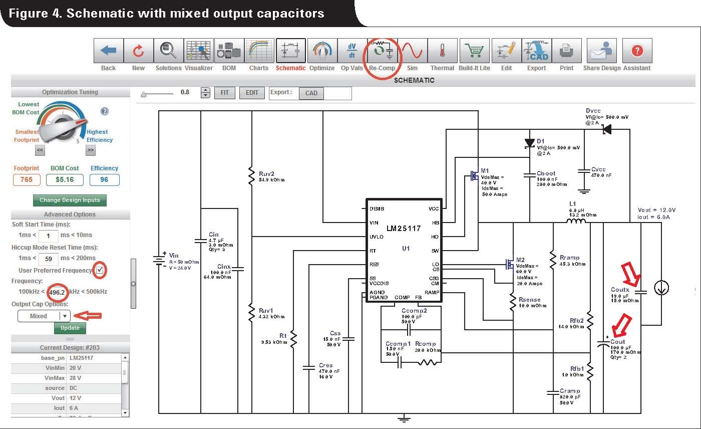
You can enter the requirements either in the WEBENCH panel or directly into the panel on the product page of the chosen regulator. For this example, the LM25117 buck controller was chosen and the input conditions were entered on the product page. After the design is started, an advanced-option section will appear on the left side as shown in Figure 4. This design needs good transient performance, so the “user preferred frequency” box was checked and “500 kHz” was entered in the box below to allow a wide loop-crossover frequency. Under the “Output Cap Options,” “Mixed” was selected and then “Update” was clicked to start a new design that allows 500 kHz and mixed output capacitors. These selections are circled in red in Figure 4.
After clicking the schematic to enlarge the view, the components on the schematic can be changed by double-clicking on the component. In this case, the inductor (L1) was double-clicked to choose a slightly lower cost option. Each output capacitor (red arrows in Figure 4) was changed for the desired mix of electrolytic and ceramic capacitors. COUT was changed to two 100-µF electrolytic capacitors from the tool’s database and COUTX to a ceramic capacitor. The database has several suitable ceramic capacitors. However, the tool did not have the 22-µF ceramic capacitor shown in Figures 2 and 3. The COUTX capacitor was double-clicked and then “Create Custom Part” (bottom of window) was selected. A 19-µF ceramic was substituted for the 22-µF typical value to adjust for reduced capacitance at the 12-V bias voltage and 15 mW was entered for ESR, which adds a little resistance for traces.
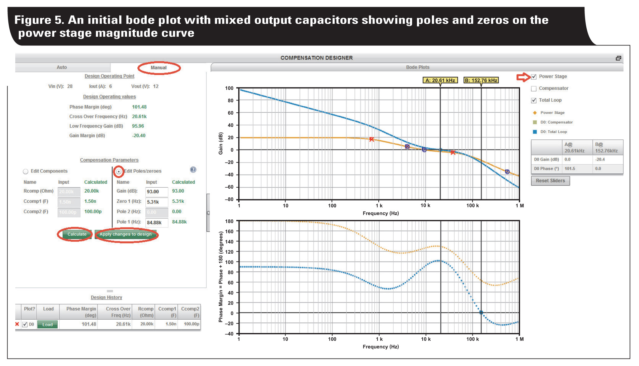
After changing the output capacitors, the “Re-Comp” button (Figure 4, circled in red) was clicked to see the bode plot and change the compensation.The blue curves in Figure 5 show the total loop magnitude and phase, while the orange curves show the power stage response. The tool marks the pole and zero locations of the power stage with the mixed output-capacitor design and the power-stage gain curve.
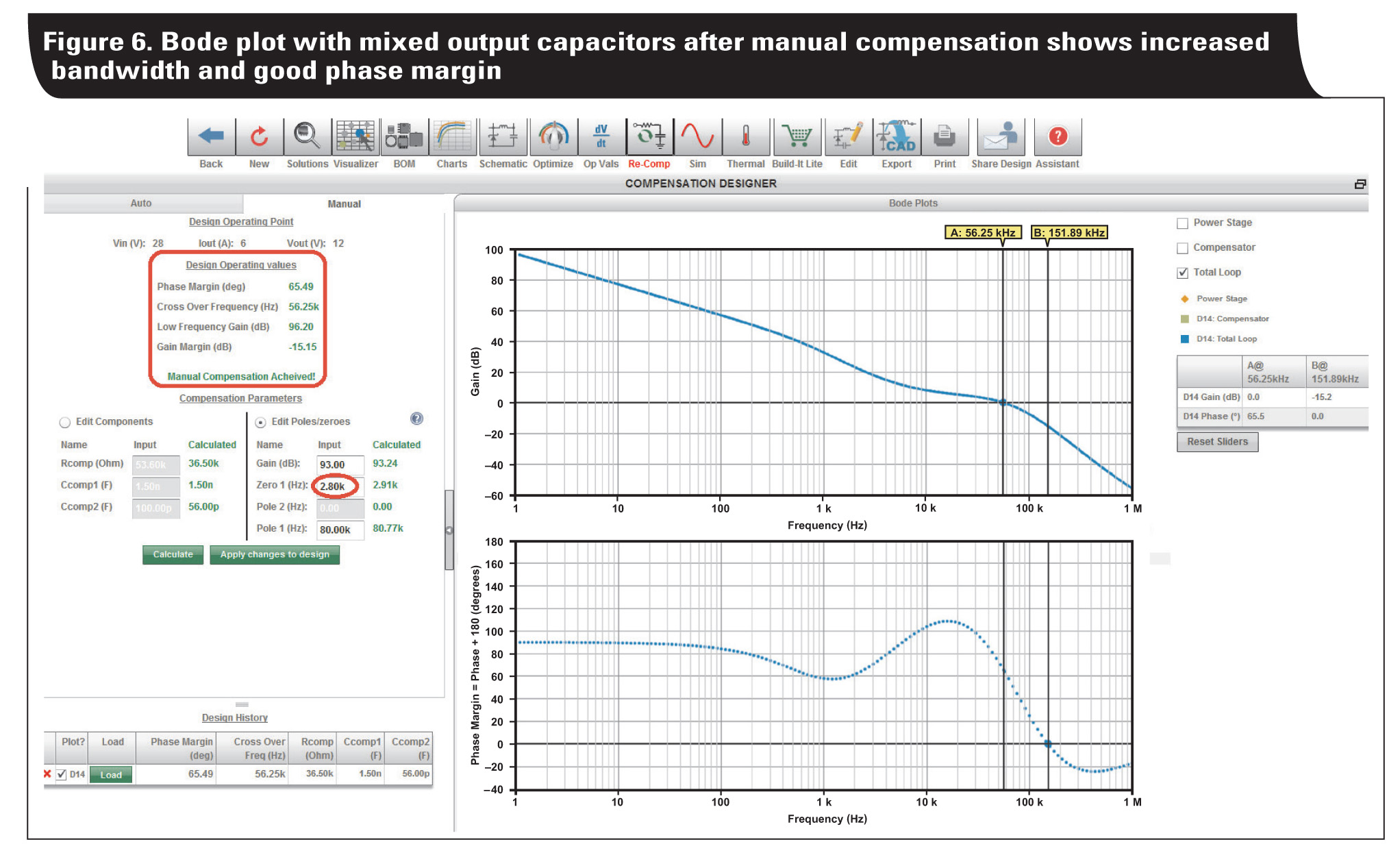
Stability of the selected design is sufficient, but the goal was to get a wider crossover frequency. The WEBENCH Compensation Designer allows auto compensation with the option to select a cross-over frequency, gain margin, and phase-margin ranges. In this example, however, manual compensation was selected for control of the compensation poles and zeroes instead. The “Edit Poles/ Zeroes” option allowed the compensation poles and zeroes to be moved and component values automatically changed to meet the pole/zero locations. “Zero1” was decreased from 5.3 kHz to 2.8 kHz to increase the crossover frequency and remove some of the dip in phase at 1 kHz. Pole1 was acceptable to stay near its original frequency of 80 kHz.
Moving the compensation zero to 2.8 kHz increased the crossover frequency from 21 kHz to 56 kHz. Phase margin was reduced to 65 degrees and the gain margin to 15 dB, which is still a very stable design. The stability results are circled in Figure 6. Selecting the “Apply Changes to Design” button updates the schematic.
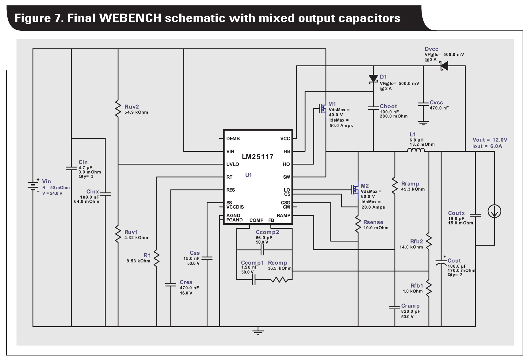
The final schematic is shown in Figure 7. If the system does not already have bulk decoupling, an electrolytic should be added to the input for additional bulk capacitance. If needed, the 47-nF capacitor shown in Figure 3 could be added to the output to reduce EMI.
Low impedance of output capacitors across frequency and a high loop-crossover frequency provide good transient response. Using both ceramic and electrolytic output capacitors minimizes capacitor impedance across frequency. Ceramic capacitors are best for high frequency and large-value electrolytic capacitors are good for low frequency. Completing a stable design with mixed output capacitors using a pen and paper is challenging, but WEBENCH Power Designer makes it easy to design with mixed capacitors and also re-compensate for improved performance.
Michael Score is a Senior Technical Staff member, Field Applications Engineering with Texas Instruments. Click here for the a pdf of the article as it appeared in TI’s Analog Applications Journal 3Q 2015.


Leave a Reply