Determining the durability and reliability of power electronics starts with strategies for estimating the lifespan.
In mechanics, it is obvious that moving parts wear under friction, and the countermeasure is also clear: lubrication. Lubrication reduces friction and thus wear, or vice versa, extending service life. Power electronic components are also subject to wear. Since this wear is based on thermomechanical processes that remain hidden from the eye, a frequently recurring set of questions arises:
- What is the reason that power semiconductors are limited in their service life?
- What is the biggest influencing factor?
- How do you create a robust estimate of how long a semiconductor will last? The first two questions can be quickly answered by looking at a power semiconductor’s structure, as given shown in Figure 1.
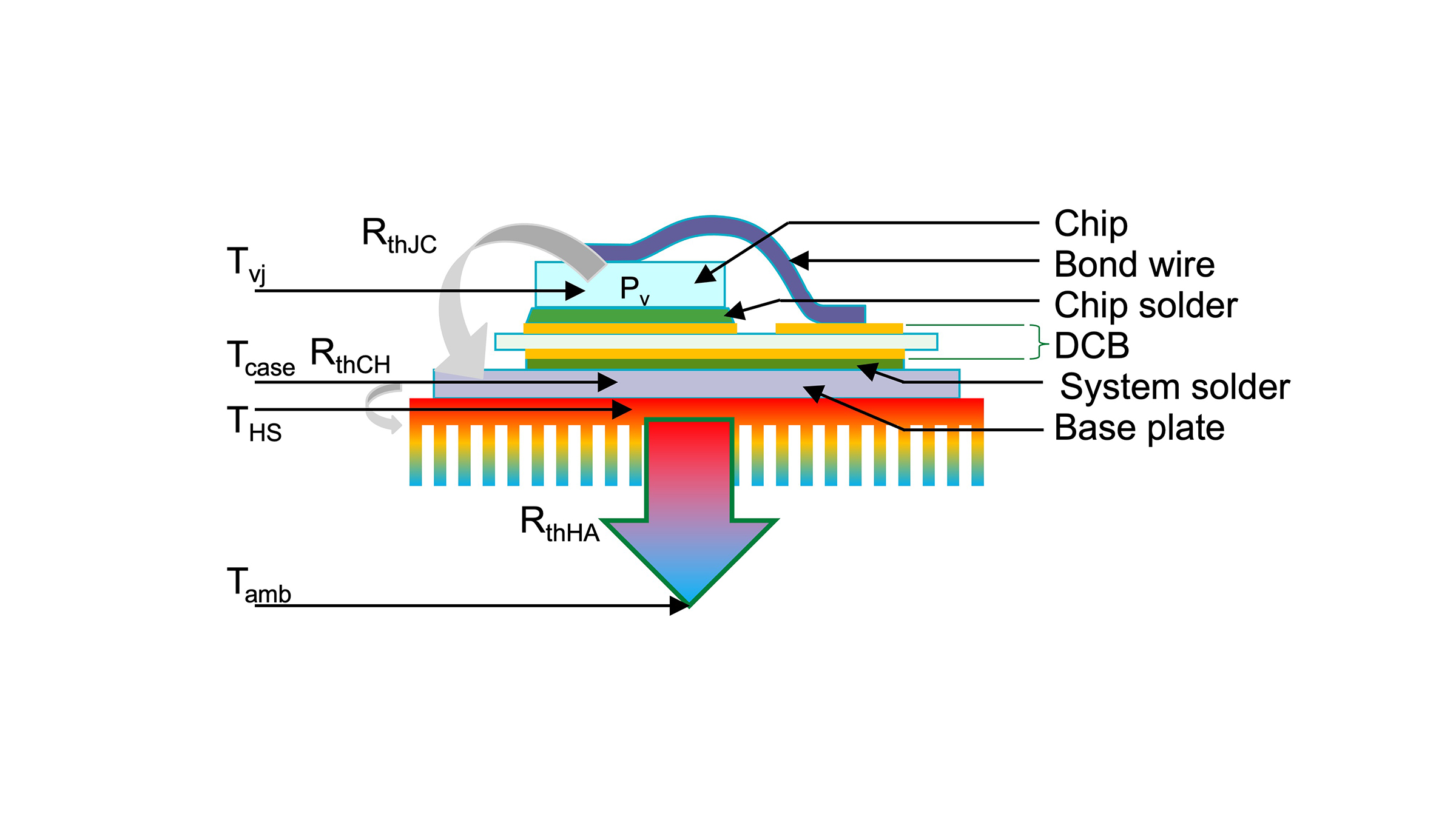
The structure consists of a ceramic laminated with copper on both sides, the so-called DCB (Direct Copper Bonding).
The DCB carries the semiconductor on its structured upper side. The chip itself is soldered on and connected to the surrounding structures by means of bond- wires. This structure is attached, also by soldering, to a base plate, which may be omitted for smaller components.
Figure 1 depicts how the heat generated by the chip is dissipated to the environment via the resulting thermal resistances. In the process, all layers of the structure heat up at different temperature levels.
Modern semiconductors now reach operating temperatures of up to 175°C, but heat sinks should not exceed a temperature of 85°C for reasons of burn hazard.
Liquid coldplates usually have a maximum inlet temperature of 65°C.
Since all the materials involved expand differently when heated, mechanical stresses arise between the layers as shear forces. These recurring stresses eventually lead to disruption (delamination) of the structure if the exposure time is long enough.
Especially In the case of bond-wires, another effect occurs. Their ends are firmly bonded to the underlying surfaces, but their length changes when the temperature changes. Because of the low thermal capacities, this heating takes place in the time range of a few seconds.
The length expansion causes microscopic movements and tiny angular changes at the mounting points and bends the wire. At the same time, the aluminum of the bonding wire expands differently than the crystalline structure of the chip; mechanical stresses occur between the so-called bond foot and the chip surface, which sooner or later leads to (dis) failure of the bond.
From the description of the failure mechanisms, the answer to the question of the driving parameter is immediately apparent: it is the temperature swing.
A power semiconductor can efficiently operate at a constant high temperature for extremely long periods. The same device, however, can fail quickly if the temperature constantly fluctuates by a high amount. The last and most important question about voltage and mechanical requirements, if any a robust lifetime prediction is not so easily answered. It is like asking the question, “How long does a car last?”
It is easy to see that a vehicle can easily be used for 20 years as a second car with only occasional use, but if used as a cab, its life is limited to 2-4 years. In fact, it may not be suitable for use as a horse-trailer tractor.
The key to answering the power semiconductor lifetime question, like that of the car, lies in the load profile of the application.
In principle, there is such a load profile for every electrotechnical application. This profile can be a forecast of solar radiation for installing a photovoltaic system or the local wind profile for the construction site of a wind turbine. Likewise, torque curves on machine tools, driving profiles of mobile applications, or charging curves for batteries come into question. Ideally, there is a precisely known individual profile. More often, however, generic profiles that describe the application in its expected typical use are found.
A well-known example of such a generic profile is represented by the driving cycles that underlie the determination of the fuel demand of commercial vehicles.
The procedure’s core is always the solution of a linear equation, which also results from Figure 1. What is always sought is the chip temperature Tvj. This value is obtained from the power dissipation and the sum of the thermal resistances as a markup on the ambient temperature as seen in this equation for chip temperature (Figure 2).

Regardless of the load profile, selecting a semiconductor must consider the blocking voltage and mechanical requirements, if any.
The forward calculation
The load profile data can always be translated into a current profile, which allows a first selection of a power semiconductor.
The expected power losses can be calculated using the electrical parameters current and voltage and the characteristics of the selected semiconductor. If the cooling is known with sufficient accuracy, or at least a maximum permissible heat sink temperature, the temperature swings at the chip’s junction can be estimated. As you can see in Figure 3, there are two steps describing how to get from load profile to temperature swing.

For technology series, semiconductor manufacturers have curves that correlate the possible number of cycles and the associated temperature swings. For Littelfuse IGBT modules based on solder-bond technology, the curve is shown in Figure 4.
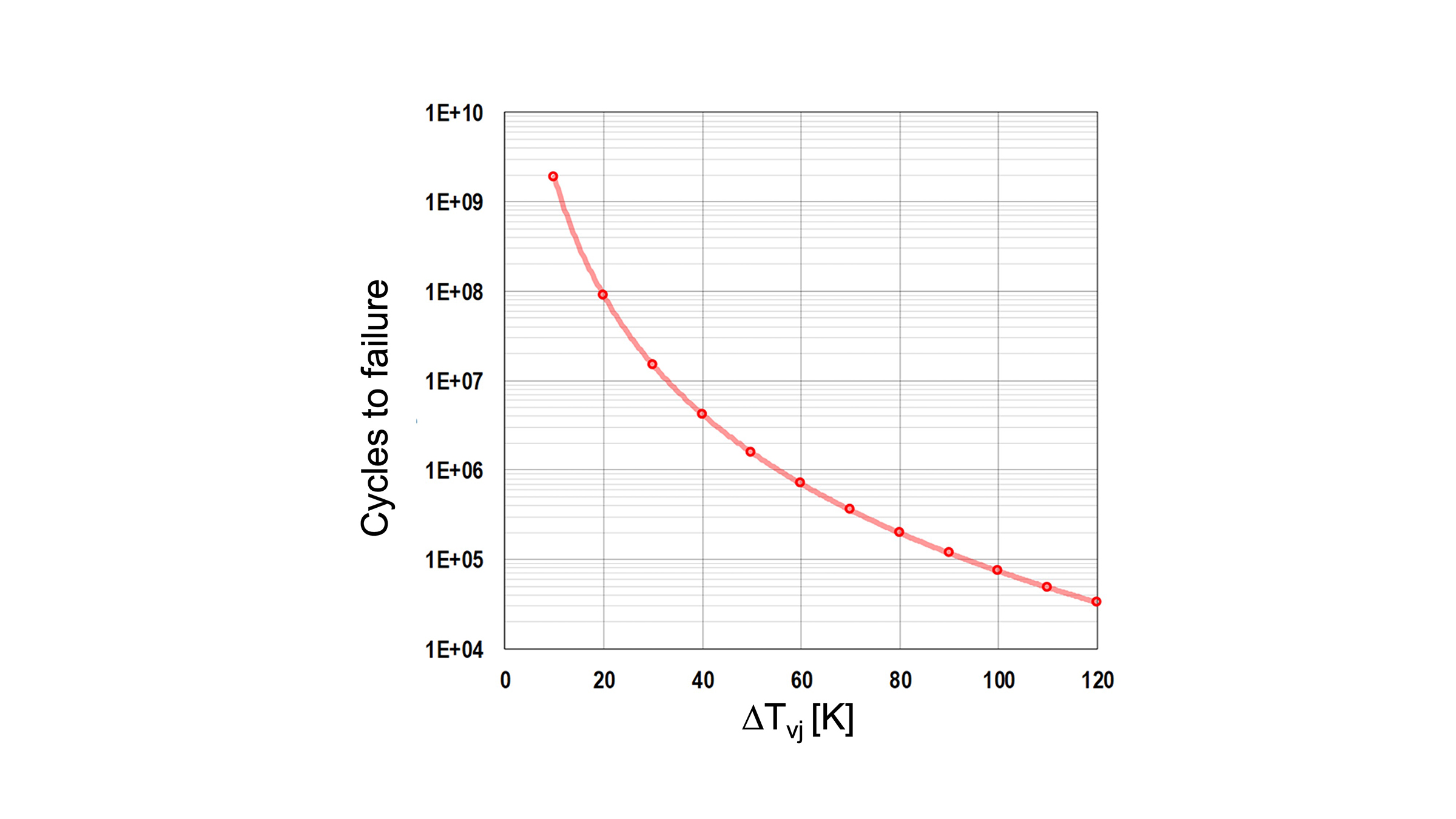
The design is successful if the load profile, temperature range, service life requirements, and number of cycles match.
If the service life is too short, various adjusting screws can be used to reduce the temperature swing:
- Selection of a more powerful semiconductor in the same package
- Selection of a design with lower thermal resistance
- Use of a heat sink with better heat dissipation
- Change from air cooling to liquid cooling
- Reduction of the switching frequency to reduce dynamic losses
Conversely, these levers can also help if the lifetime is too long. Although a reasonable reserve is to be welcomed, a service life prediction that is far too high can also be a sign of an oversized and, therefore, overly costly design.
The backward calculation
The load profile and the expected lifetime give a first impression of how many load cycles the semiconductor must withstand in the given application. Using the curve for cyclic load N=∫(DT) from Figure 4, an estimate of the tolerable temperature swing can be made from this.
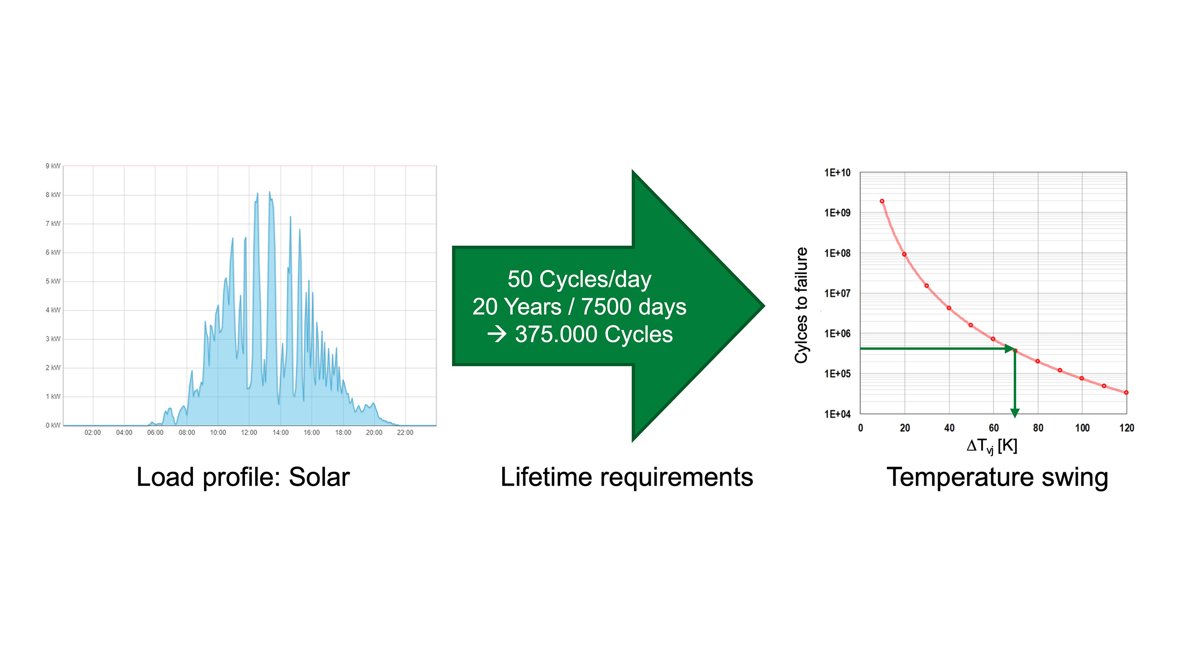
Figure 5 shows how the maximum temperature deviation can be estimated directly from the load profile. The temperature swing of 70K resulting from the diagram allows a maximum heat sink temperature of 55°C when a maximum of 125°C applies to the chip temperature. Selecting a suitable semiconductor is then based on thermal resistance and power dissipation. Again, iteration is often necessary to determine the best matching component or to adjust the result in conjunction with a variation of the heat sink. The relationship taken from Figure 5 already leads to a reasonably conservative design. The assumed 50 cycles per day include a comfortable margin. Additionally, the selected daily profile represents an unfavorable case that will not occur this way on most days. If the cost situation permits, the conservative design is to be preferred.


Thanks for the explanation of the “wear-out” mechanism of semiconductors that have internal leads. I wonder how the heating and cooling affects individual transistors and other devices that do not include bonding wires.
one person has been asserting that audio amplifiers wear out rapidly and that any over a year old are probably worn out and do not sound as good. Of course, there is no ground for discussion with those whose technical insight is less than an average donut.