Silicon-carbide MOSFETs and digital gate drivers work together to make electrified metro, subway, and other heavy transportation vehicles possible.
Nitesh Satheesh, Tomas Krecek, Perry Schugart, Xuning Zhang, Kevin Speer, Microchip Technology
 Green initiatives continue to transform power electronic system designs in industrial, aerospace, and defense applications, and especially the transportation sector. Silicon Carbide (SiC) technology is at the center of this trend, delivering new capabilities for cutting greenhouse gas (GHG) emissions by electrifying a broad and growing range of vehicles and aircraft.
SiC devices enable smaller, lighter, and more efficient electrical alternatives to aircraft pneumatics and hydraulics systems for powering on-board alternators, actuators, and Auxiliary Power Units (APUs). They also reduce the maintenance requirements for these systems. But the most prominent showcase for SiC technology is the mission to electrify commercial transportation vehicles which are among the world’s biggest sources of GHG emissions. With the arrival of 1,700-V MOSFETs and configurable digital gate driving technology, today’s SiC devices enable designers to extract the most productivity from these systems while dissipating the least amount of energy.
Moving to 1,700-V MOSFETs has extended SiC technology’s power conversion benefits to electrified commercial and heavy-duty vehicles as well as to light rail traction and auxiliary power. The devices are enabling the automotive powertrain of today and the future and are quickly replacing older silicon MOSFETs and Insulated-Gate Bipolar Transistors (IGBTs). They meet the high power and voltage requirements of big CO2-equivalent GHG emissions emitters including buses, rail, medium- and heavy-duty trucks, and the charging infrastructure. They also deliver much higher system efficiency and reliability than silicon MOSFETs and IGBTs, enabling designers to reduce the size of auxiliary power units (APUs) and other key vehicle systems.
Today’s 1,700-V SiC devices reduce switching losses to a tiny fraction of what silicon IGBTs exhibit. This enables designers to boost switching frequency and shrink the size of the power converter. The devices have no knee voltage, unlike IGBTs, so conduction losses are also lower for systems such as transportation APUs that operate under “light load conditions” – i.e., they open and shut train doors that spend most of their time closed and not drawing power. A vast array of applications operate at light load across the majority of their service lifetimes. Designers can make use of SiC MOSFET low switching and conduction losses to eliminate a variety of thermal management measures such as heat sinking.
The simplified circuit topology and reduced component count of today’s higher-voltage SiC MOSFETs also improve reliability while reducing costs. Their 1,700-V blocking voltage reduces power converter size and enables designers to replace three-level circuit architectures with a much less complex two-level circuit—that is, two semiconductor devices between input and output rather than three. This halves device count – or more – while streamlining control.
SiC MOSFET considerations
When choosing SiC MOSFETS for heavy-duty transportation vehicles and other multi-megawatt applications, designers must consider several important factors. Among these is whether to use modular devices based on a basic unit cell (also known as a power electronics building block or sub-module).
Historically, the power semiconductor devices used in the unit cells have been 1,200 to 1,700-V silicon IGBTs. Much as in lower power applications, the deployment of 1,700-V SiC MOSFETs at the unit cell level extends power handling capability and electrical performance. Because 1,700-V SiC MOSFETs have much lower switching losses, it becomes possible to boost switching frequency and drastically reduce the size of each unit cell. Moreover, the high 1,700-V blocking voltage reduces the number of unit cells needed for a given dc link voltage, which ultimately heightens system reliability while slashing cost.

Designers should also evaluate the SiC MOSFET intrinsic body diode. Devices should show no perceptible shift in tests of pre- to post-stress ON-state drain–source resistance (RDSon). This point is critical for ensuring the MOSFET will not degrade after many hours of constant forward current stress as it conducts reverse current and commutates any remaining energy after a switching cycle. Designers must carefully review SiC MOSFET test results because devices from different suppliers can exhibit substantial variations. Many show at least some level of degradation while others may even become unstable. Choosing a SiC MOSFET that will not degrade eliminates the need for an external antiparallel diode and associated die cost and power module real estate.
There still may be challenges associated with varying levels of potentially inconsistent body diode performance – for some devices more than others. These inconsistencies can be resolved by adjusting the SiC MOSFET turn-on parameters using configurable digital gate drivers. These same drivers also are used to mitigate the secondary effects arising from the faster switching speeds of SiC MOSFETs. These effects can include noise and electromagnetic interference (EMI) as well as limited short-circuit-withstand time and overvoltage caused by parasitic inductance and overheating. Configurable digital gate driving has become the key to unleashing the full capability of SiC technology.
Configurable digital gate drivers have been designed specifically to mitigate the secondary effects of SiC MOSFET faster switching speeds. Besides cutting drain-source voltage (VDS) overshoots by up to 80% as compared to the traditional analog approach, they halve switching losses and reduce time to market by up to six months. They make it possible to source/sink up to 20 A of peak current and provide an isolated dc/dc converter with a low-capacitance isolation barrier that can be used for pulse-width modulation signals and fault feedback.
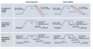
Configurable digital gate drivers also provide robust fault monitoring and detection while delivering independent short-circuit response. They offer much more precise MOSFET turn-on/turn-off control than traditional analog gate drivers, which only control turn-off slope through gate resistors for normal and short-circuit situations. Even when standard analog gate drivers are adapted for use with SiC MOSFETs, they cannot deliver these capabilities.
Augmented switching capabilities via configurable digital gate drivers enable designers to significantly reduce development time. Designers can explore configurations and re-use them for different gate driver parameters such as gate switching profiles, system-critical monitors, and controller interface settings. Thus designers can quickly tailor gate drivers to a variety of applications without any hardware changes. Control parameters can be modified at any point in the design process, and designers also can change switching profiles in the field as application conditions require and/or SiC MOSFETs degrade.
These augmented switching capabilities continue to evolve. Digital gate driving now provides up to two turn-on control steps compared to the single step of traditional analog drivers, and up to three turn-off control levels. The multiple steps provide a “soft landing” during turn-off that is much like tapping a foot on an antilock system’s brakes. The addition of a fourth short-circuit setting level provides the opportunity for even more precise control over the secondary effect of SiC switching speeds. It also helps address overshoot, ringing and turn-off energy, among other variables. These capabilities give designers the combination of faster switching and more granular and dynamic, multi-step turn-on and turn-off control that will enable them to meet the increasing demands of SiC applications.
One example is motor control. A too-high rate-of-change of voltage (dV/dt) shortens motor life expectancy and correspondingly boosts warranty costs. Until higher-frequency motors are available, the only way to solve this problem with analog gate drivers is to slow SiC switching speed at the expense of efficiency. Only with the configurable augmented turn-on capabilities of digital gate drivers can dV/dt be optimized.
Use of a comprehensive SiC ecosystem offers a direct path from evaluation to production. Key elements include a gate driver core, module adapter boards, an SP6LI low-inductance power module, mounting hardware, and connectors to the thermistor and dc voltage. Programming kits should be provided for the configurable software.
The module adapter boards are particularly important. They enable designers to quickly configure and re-use gate driver turn-on/turn-off voltages. This re-use can take place across many different suppliers’ SiC MOSFETs with a variety of positive or negative voltage ranges, without requiring any redesign, even if the SiC MOSFET previously used an analog gate driver. Simply reconfiguring the digital gate driver enables designers to immediately move into production. Meanwhile they can continue mixing and matching gate driver cores and module adapter boards and follow the same accelerated path to production. They can begin testing immediately with an SP6LI low-inductance power module connected to a laptop computer and a phase leg.
The combination of 1,700-V SiC MOSFETs with digital gate driving technology has already had an impact on the “electrification of everything” and, more specifically, heavy-duty transportation vehicles. It has enabled SiC technology to support vehicle power conversion needs while improving efficiency and reliability. In addition, the augmented switching capabilities provided by configurable digital gate drivers is speeding and simplifying the path from design to production. Use of these drivers also create new capabilities including the ability to change switching profiles in the field as application conditions require and/or as SiC MOSFETs degrade.
One of the most welcome benefits for designers is that the use of configurable digital gate driving with these devices eliminates the laborious process of soldering gate resistors onto a board to change behavioral parameters. All of this can now take place via keystrokes, accelerating the Electrification of Everything.


Leave a Reply