One key factor: Determining the nuances of how capacitors handle expected ripple currents.
Sam G. Parler, Jr., P.E. Cornell Dubilier
Examine a dc link capacitor’s ac ripple current and you’ll realize it arises from two main contributors: the incoming current from the energy source and the current drawn by the inverter. Of course, capacitors cannot pass dc current; thus, dc current only flows from the source to the inverter, bypassing the capacitor. Power factor correction (PFC) in the converter and/or regenerative energy flow in certain inverter topologies can complicate matters. But in all cases, instantaneous current is conserved at the three-current node of the dc link capacitor connection. Although some cancellation can arise between the ac components of the source current and the inverter current, it is usually a good approximation or at least conservative to estimate the capacitor’s RMS ripple current as
I2capRMS ~ I2sourceRMS + I2inverterRMS (1)
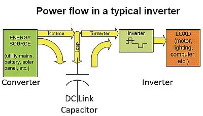
This relationship is usually valid because the converter stage generally has much lower frequency ripple current content than the inverter stage. The approach to the analysis we’ll use starts by examining the converter stage alone and treating the inverter as a load with a fixed power dissipation or resistance.
To simplify things and generalize the conclusions, we’ll implement a Per-Unit (PU) analysis. (As a quick review, a per-unit system expresses quantities as fractions of a defined base unit quantity. This simplifies calculations because quantities expressed as per-unit do not change when they are referred from one side of a transformer to the other.) We’ll use as a base the load power drawn by the inverter, assuming a conserved quantity, power, P; and a mains frequency, f. This is basically the ideal dc power delivered to a load resistor, so the base voltage is equal to the peak voltage at zero ripple voltage. The relationships are:
Vbase = Vdc(Peak), Ibase = P/Vbase, Rbase = V2base/P, Lbase = V2base/2πfP, Cbase = P/2πfV2base

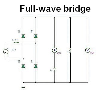
Now consider a rectified single-phase 50-Hz mains with ideal diodes. Such “linear” power supply schemes can produce a high ripple current in the dc link capacitor which here serves as a filter capacitor. The current pulses charging the capacitor when the diodes are forward-biased are generally much shorter than the time over which the capacitor discharges into the load. From the principle of charge conservation in a capacitor, these pulses are therefore quite a bit higher in amplitude than the load current. The high pulses usually result in the capacitor RMS ripple current exceeding the dc current delivered to the load.
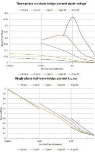
Most power supply designers want a peak-to-peak ripple voltage below 5% and usually limit line inductance to about 5% per-unit. A Spice analysis reveals that a single-phase full-wave bridge requires a lot of capacitance, on the order of 40 PU or more. As long as some line inductance (such as 1% per-unit) is incorporated, the RMS ripple current is relatively insensitive to the level of capacitance. Plots of capacitor ripple current reveal only few frequency components at two, four, and six times the line frequency.
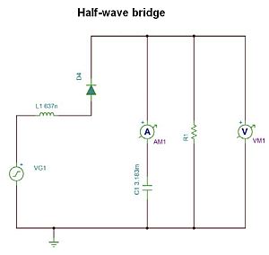
Now consider a half-wave bridge. It is even more demanding on a per-unit basis than a full-wave bridge, with regard to the capacitor ac RMS ripple current and peak-to-peak ripple voltage. It takes a capacitance on the order of 100 PU or more to realize a peak-to-peak ripple voltage of less than 5%–It’s probably cheaper to just add three diodes! Here, it takes more line inductance–several percent per unit–to lower the RMS ripple current to a modest level. The frequency content of the capacitor ripple current is nearly zero at dc (0 Hz) as it must be. There are only a few frequency components at half the frequencies of the full-wave bridge at one, two, and three times the line frequency, rolling off rapidly.

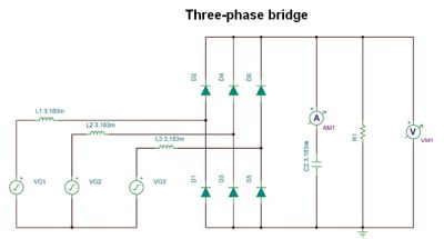
Further consider three-phase, six-diode rectifiers. The per-unit inductance is in each leg of the three-phase lines. We keep the same base units as for single-phase so the comparisons will be on the nominal power delivered to the resistive load at its nominal peak voltage. Such a rectified waveform, without L and C, would have a ripple voltage below 1-√3/2 ≈ 0.134 per-unit, as this is the maximum droop from the peaks of the three 120º phase-shifted, overlapping sinusoidal mains-voltage rectified waveforms.
We observe that with only 1.5% line inductance, ripple voltage can be less than 5% with a capacitance of only four per-unit, as compared to 40 for a single-phase full-wave bridge. However, even for the three-phase, six-diode rectifier, a Cpu below four isn’t advisable for normal values of Lpu because enormous ripple voltage occurs at 1 and 2 PU. This is due to the LC ringing.
Capacitor ESR drops with rising frequency. Instead of ripple current components at small multiples of the utility mains frequency, the peaks on the spectral plot are now at 6, 12, and 18 times the mains frequency. The peaks are at multiples of 25 Hz, and thus the energy bands are at all integer multiples of six times the 50 Hz mains frequency, decaying rapidly.
The rectified-mains analysis reveals the energy source to be a sequence of current pulses applied to the capacitor. This suggests that a similar approach may be applied to the analysis of the inverter input current, which draws a sequence of pulses from the dc link capacitor. Both of these sets of pulses will cause voltage ripple as well as ripple current and its attendant heating.
As far as the effect on capacitor ripple current and ripple voltage, the main difference between these two distinct sets of pulses, energy source versus inverter sink, is the range of frequencies involved. Typically, the rectified mains and its harmonics are less than 2 kHz, while the inverter switching frequency and its harmonics are usually above 2 kHz.
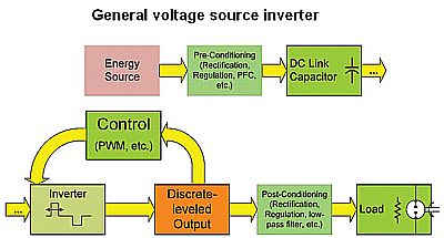
No rule states that the energy source must be diode-rectified. In fact, it could be chopped with IGBTs or SiC switches. Circuits that accomplish power factor correction, bi-directional energy flow (e.g. regenerative braking), etc. generally operate this way.
Ultimately the overall analysis of the capacitor ripple current and voltage will involve the superposition of the current flows at its connection node. In general, the inverter stage uses solid-state switches to chop its dc voltage input to create a digital-looking (multilevel) or an even simpler binary (two-level) output voltage waveform, depending upon how many “levels” (discrete voltage values, varying from two to six or more levels) the PWM topology incorporates. (For this reason, these circuits were once referred to as choppers and sometimes still are, especially for dc-dc converters. More formally they are called PWMs, pulse-width modulators.)

The unfiltered PWM output voltage is never a true sine wave. But when driving an inductive load such as a motor, the current will tend to be proportional to the time integral of the PWM voltage waveform, whose modulation scheme is designed so the Webers (volt-seconds) of these pulses will produce approximately a sinusoidal current (since, for an inductor L, IL= ∫ v dt/L). And for applications such as a UPS requiring something close to a sinusoidal voltage, an LC or ferro-resonant filter after the PWM stage can effectively integrate and low-pass-filter the voltage waveform.

The PWM control/modulation scheme can affect capacitor heating. But usually, power supply designers primarily want to meet goals involving efficiency, cost, size, reliability, total harmonic distortion limits, and sometimes input power factor limits. So minimization of capacitor losses isn’t always the highest priority. Still, it is good to investigate and quantify the relative impact of various factors affecting the capacitor stress.
There are many inverter PWM switching and control schemes. Some are carrier-based, some are not. We will consider a somewhat simplified scheme to demonstrate how a typical inverter input influences the dc-link capacitor ripple current and ripple voltage.
The scheme we will consider is carrier-based sinusoidal PWM, also known as SPWM. Here, the sinusoidal ac voltage is compared with a high-frequency triangular carrier wave in real time to determine switching states for each pole in the inverter, thereby generating a binary PWM signal. The triangle wave is a fixed-frequency carrier with a repetition frequency equal to the inverter switching frequency. The amplitude of the sinusoidal reference signal as a factor of the amplitude of the reference signal is known as the modulation index, m.
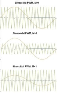
Now again consider the three-phase, six-diode rectified 50-Hz mains. Instead of a fixed-resistance load, suppose there is an inductive load with a series resistor. Further suppose we drive this load with a mathematically generated SPWM source voltage.
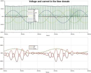
The spectral plot of the inverter input current shows a large dc (0 Hz) component as well as 40, 80, and slight 120 Hz peaks, which are multiples of the 40 Hz single-phase motor drive output frequency. However, there is no sign of the 300-Hz rectified mains current component. On the other hand, the capacitor ripple current shows no dc component but possesses a 40-Hz output current and its multiples, along with a large 300-Hz component due to the rectified three-phase 50 Hz mains.
Also, the capacitor’s ripple current spectrum contains two sidebands straddling the 300 Hz component; these are at 300 ± 40 Hz = 260 and 340 Hz, typical of the modulated interaction between the mains input and the motor drive output. Note that the existence of such modulated sidebands suggests the possibility that inverter schemes with multiple switching, rectification, and ac-output frequencies can potentially produce ripple current components at frequencies below any of the fundamental frequencies associated with these components, thereby potentially increasing capacitor losses.
Capacitor ESR can be modeled approximately as having two terms, a first-term Ro that doesn’t vary with frequency, and a second term Rd which arises from the dielectric loss angle. The series resistance associated with dielectric loss varies approximately in direct proportion to 1/f over an extremely broad frequency range:
ESR=Ro+Rd (f) = Ro+DXc = Ro+D/2πfC (2)
The second term is equal to the dissipation factor D multiplied by the capacitive reactance. Thus, ESR overall tends to drop monotonically with rising frequency. The dielectric resistance is directly proportional to D and inversely proportional to the product of frequency and capacitance. Thus for a given RMS component magnitude, the low-frequency components of ripple current cause more heating than the high-frequency components.
Spectral analysis and Joule heating
Consider the following hypothesis about the current drawn by the inverter from the capacitor: For a given ac RMS value and pulse duty, the dielectric loss component of the dc link capacitor is a strong function of the inverter switching frequency and current pulse spacing, but not of the exact pulse shape.
To evaluate the hypothesis, we will examine five pulse-current waveforms, each at a repetition frequency of 1 kHz (i.e. a 1-msec period) and having a value of 33.3 A RMS.
First, consider a 100-A, 100-µsec pulse. It has a large fundamental component at the 1 kHz rep rate. Because capacitor ESR has a 1/f term, the dielectric loss would be half as much at 2 kHz as at 1 kHz. This shows that the dielectric loss is a strong function of the switching frequency. With a 130-µF capacitor, a dielectric loss tangent of D = 2% yields a power loss of 11.9 W for this waveform.
Next, suppose the RMS value, repetition frequency, and pulse width remain the same, but the pulse shape changes from flat-top to sloped and then to sawtooth–from completely flat-topped to progressively more sloped. Different as the waveforms appear in the time domain, their spectra are similar, and the reference capacitor losses for the three cases are, respectively, 11.9, 11.7, and 10.1 W. This shows that the dielectric loss is not a strong function of the exact pulse shape for a given RMS value and pulse duty.
Finally, consider the spectrum and dielectric heating from a 100-µsec-wide flat-top pulse with an inverted twin pulse in two configurations: first, in close proximity and then separated by some distance. The contiguous-pulse arrangement depresses the 1-kHz fundamental harmonic which results in a dielectric heating of the reference capacitor of only 7.46 W. Equal/maximum inter-pulse spacing within the 1-msec period results only in odd harmonics with a pronounced, dielectric-loss-inducing fundamental. At 14.43 W, the power loss in the reference capacitor is nearly twice that of the contiguous pulse pair. This shows that the dielectric loss component of the dc link capacitor is a strong function of the inverter current pulse spacing.
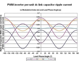
For the case of a PWM inverter with a balanced three-phase output, there is an expression that gives a good estimate of the capacitor ripple current in terms of both the previously discussed modulation index m and the load’s phase current and phase angle φ. It is generally accurate within several percent for most PWM inverter modulation schemes with three-phase ac outputs:

Note the expression is the ratio of the capacitor RMS current to the line output current from the inverter to the load. Note also that it is independent of the inverter switching frequency.
It appears that, for most inverter applications, the ripple voltage can be estimated using a per-unit analysis to pick a range of possible capacitances versus the design’s operating voltage, power level, and frequency. However, are any ride-through requirements may force the use of a higher capacitance level.
The capacitor voltage rating must exceed the worst-case peak bus voltage as might arise under “high-line” mains conditions, maximum solar-panel output voltage, etc. Low-ESR aluminum electrolytic capacitors are rated only up to 500 Vdc, so they may need to be connected in series with balancing resistors. Film capacitors are rated to much higher voltages than aluminum electrolytic capacitors and generally do not require a series connection. Aluminum electrolytic capacitors are less expensive per unit of nameplate energy, but they don’t handle as much ripple current per unit of stored energy, so the ripple current handling needs to be investigated.
Now consider three-phase inverters at any dc bus voltage. For films and electrolytics, respectively, a rule of thumb is that about five (film) and 50 (electrolytic) mC of capacitor nameplate CV rating (i.e. its volumetric efficiency) is necessary per Amp of ripple current. For example, on a 10-hp motor drive with a 700-Vdc bus, a capacitor ripple current of 7 A RMS would need a 50-µF film or a 500-µF aluminum electrolytic capacitor. The probable embodiment would be a single 50-µF 800-Vdc film vs two 1,000 µF 400-V aluminum electrolytic capacitors in series. These rules of thumb may need to be tripled or more for single-phase high-impedance inputs or for large ride-through requirements.
To examine the per-unit capacitance of this arrangement we can rearrange the base equations. But we shouldn’t use the capacitor voltage and ripple current; rather, we should use the motor line voltage and full-load current. Suppose the 10-hp motor is driven with 460 V and 12.4 A. Using a three-phase base power of √3VLINEILINE = 9,880 VA results in per-unit capacitance values of Cpu=3.36 for the electrolytic and 0.336 for the film capacitor.
Capacitor lifetime and failure rates are exponential functions of temperature and thus of ripple current. Consequently, the ripple current stress on the dc link capacitor is critical and must be managed carefully and conservatively. With the minimum capacitance and voltage rating chosen as discussed above, the next step is to calculate the total ripple current.
A rule of thumb is to choose a capacitor whose rated ripple current at high-temperature, short-duration life-test conditions is in the ballpark of the total calculated dc link ripple current. The rated “load test” current often is accompanied by tables of so-called “ripple multipliers” that apply for higher application frequencies or lower ambient temperature and derated dc voltage. But be aware that applying these multipliers to the rated ripple current reduces the capacitor lifetime to its nominal test duration, which is typically only 5 to 10 thousand hours. So, it’s a better first approximation to start with candidates whose nominal ripple current rating is close to the actual application ripple current, at least until you can perform thermal and lifetime calculations.
The thermal analysis proceeds by partitioning the ripple current into two frequency bins per equation (1). The first bin constitutes the lower frequencies at the appropriate multiple of the mains frequency (depending upon the number of phases and upon the rectification or chopping scheme). The higher frequency bin is at the inverter switching frequency per equation (3) if a balanced three-phase PWM inverter scheme is applicable. Otherwise, the inverter input current and dc link current must be calculated or modeled.
This method of ripple current analysis should be inherently somewhat conservative for two reasons. First, there can be some cancellation between ISOURCE, AC, RMS, and IINVERTER, AC, RMS. Consequently, ICAP, RMS may not be fully equal to the RSS (root sum of squares) value of these two ripple components. The second reason for conservatism is that the capacitor ESR generally drops with rising frequency because its dielectric loss component is proportional to the capacitive reactance. This analysis method proposes that the fundamental components of these two contributions be used in the thermal analysis, so the ESR estimate should be slightly higher than in actual practice.
References
Application guides for aluminum electrolytic and power film capacitors
Core-temperature, lifetime calculators, Spice model code generators


Leave a Reply